5G Ushers in a New Era of Wireless Test
5G requires new test methods to ensure the viable commercialization of 5G products and solutions across many industries and applications.

As 5G design test cases grow in number and complexity, engineering teams must streamline to hit aggressive market deadlines. In collaboration with 5G market leaders, NI has developed a modern lab approach that drives engineering efficiency. By combining fast, reliable, and open measurement software with a modular workbench of tightly synchronized instrumentation—from precision DC to wideband RF—we’ve unlocked powerful engineering workflows across lab roles, from interactive bring-up and debug to extensive automated validation and characterization.
FEATURED SOLUTION
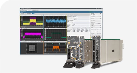
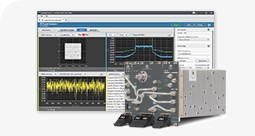
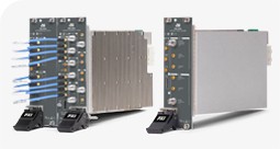
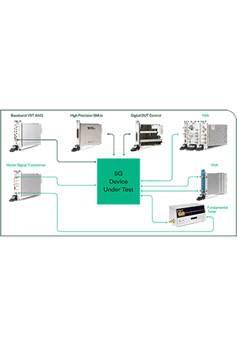
Expedite wideband 5G RF front-end bring-up, debug, and validation with NI’s powerful combination of application software and PXI instrumentation. Control DC, digital, and RF instruments with an easy-to-use GUI—no programming required. Evaluate critical RF amplifier parameters—including linearity, output power, efficiency, and modulation quality—while running the latest linearization algorithms.

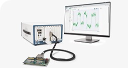
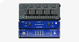
NI’s measurement-oriented software controls multichannel DC, digital, analog, and wideband RF test instruments to simplify both interactive and automated 5G design validation sequences.
Gain “Cockpit-Like” Bench Control
Improve Your Validation Workflow
Implement Subnanosecond Synchronization and Triggering
Test Multi-RF-Channel MIMO Operation
We looked at what was slowing down our characterization process in the lab, and RF measurements using traditional instruments were the most time consuming. By adopting PXI, we were able to significantly improve test throughput without sacrificing quality.
Director of Mobile 5G Business Development
Qorvo
The NI Partner Network is a global community of domain, application, and test experts working with NI to meet your needs. NI Partners are trusted solution providers, systems integrators, consultants, product developers, and services- and sales-channel experts skilled in a range of industry and application areas.

An NI Partner is a business entity independent from NI and has no agency, partnership, or joint-venture relationship with NI.