Specifications Explained: C Series Modules
Overview
The specification manuals for NI C Series modules provide the technical details necessary to determine or choose which modules are best suited for your application, and as a reference to validate performance during system development. This document provides definitions of the terminology used, in a glossary format, to illustrate the importance and relevance of each specification.
For application use and further information, please use the NI Product Documentation page to search for the required information or user manual.
Contents
- Introduction
- Understanding Specification Terminology
- Determined by the Module or the Backplane?
- Analog Subsystem Specifications
- Thermocouple Subsystem Specifications
- Digital Subsystem Specifications
- Other Specifications
- Additional Resources
Introduction
This guide is broken up into the same sections as most NI specifications manuals. Terms and definitions below are listed in alphabetical order and may occur in a different order in the specification manuals. This guide exclusively applies to C Series modules. Other NI product families such as, Multifunction DAQ 60xx, 61xx, 62xx, and 63xx families (formerly B, E, S, M, and X Series), Multifunction RIO 78xx R Series, Digital Multimeters, Scopes/Digitizers and other instruments may use different terminology or methods to derive specifications and as such, this guide should not be used as a reference for devices other than those in the cDAQ and cRIO families. While C Series modules are used with cDAQ and cRIO chassis and controllers, their specifications are not included in this guide.
This guide will use several modules as references throughout. To follow along with these specifications, look for the respective module's datasheet, available on ni.com/manuals.
Understanding Specification Terminology
First, it is important to note the categorical difference between various specifications. NI defines the capabilities and performance of its Test & Measurement instruments as either Specifications, Typical Specifications, and Characteristic or Supplemental Specifications. See your modules' datasheet for more details on which specifications are warranted or typical.
- Specifications characterize the warranted performance of the instrument within the recommended calibration interval and under the stated operating conditions.
- Typical Specifications are specifications met by the majority of the instruments within the recommended calibration interval and under the stated operating conditions. Typical specifications are not warranted.
- Characteristic or Supplemental Specifications describe basic functions and attributes of the instrument established by design or during development and not evaluated during Verification or Adjustment. They provide information that is relevant for the adequate use of the instrument that is not included in the previous definitions.
Determined by the Module or the Backplane?
Some specifications for a C Series system are designated by the modules, while others are designated by the backplane. Some specifications are also dependent on system configuration.
In general, a cDAQ chassis or controller provides timing, triggers, counters, and data transfers between modules and a host computer or the onboard controller. A cRIO controller features a real-time processor and reconfigurable FPGA for high-speed control and custom timing and triggering.
Both types of backplanes interface directly with C Series modules, which use the timing and control provided by the backplane for their inputs, outputs, or other functions. The modules perform their own acquisition and generation, and communicate that data back to the chassis which then transfers that data to the user. Some modules also contain their own signal conditioning.
All cDAQ chassis or controllers and cRIO controllers have their own safety certifications, power requirements, and other specifications. Reference your chassis' or controller's datasheet or specifications documents for specifications not found in this document..
Analog Subsystem Specifications
Analog Input
ADC resolution
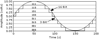
Resolution is theoretically the smallest amount of input signal change that the module or sensor can detect. The number of bits used to represent an analog signal determines the resolution of the ADC.
Example
The NI 9209 is a 24-bit module with ±10 V range , which means that lowest amplitude change that can be detected is 1.19 µV.
See Also
Noise, Idle channel noise, Input noise, or Root mean square (RMS) noise
Alias-free bandwidth
Any signal that appears in the defined alias-free bandwidth is not an aliased artifact of a signal at higher frequencies.
Example
NI 9250 specifies alias free bandwidth of 0.5 * fs, meaning that for an fs of 102.4 kS/s, the alias free bandwidth is from 0 Hz to 51.2 kHz when DC coupling mode is selected.
See Also
Bridge completion
Bridge completion refers to options provided to the user in terms of connecting Wheatstone bridge sensors, which are typically used to measure strain, to the module. The software-selectable bridge completion modes are full-bridge, half-bridge, and quarter-bridge.
Example
NI 9237 supports all three modes of bridge completion.
Additionally, the NI 9237 specifies half- and full-bridge completion as internal. This means that half- and full-bridge sensors can be connected to the module directly as there are resistors internal to the module that will complete the bridge.
The NI 9237 also specifies quarter-bridge completion as external. This means that an external resistor or a quarter-bridge completion device, such as the NI 9944 or NI 9945, is required along with the quarter-bridge to be connected to the module to complete the bridge.
See Also
Common-mode rejection ratio (CMRR)
When the same signal is seen on the positive and negative inputs of an amplifier, the CMRR specifies how much of this signal is rejected from the final output, and is typically measured in dB. An ideal amplifier will remove 100% of the common mode signal, but this is not achievable in implementation.
Example
The NI 9205 has a CMRR of 100 dB from DC up to 60 Hz. This means that it will attenuate common mode voltages by 100,000x. For example, if the signal being measured is a 5 Vpk, sine wave, and the offset or common voltage between the channel and earth ground is 5 VDC, the final output will reject or attenuate the 5 VDC input to 50 µV. CMRR is not included in accuracy derivations and should be accounted for separately if the signal measured contains common mode voltages.
IEPE compliance voltage
IEPE refers to a type of transducer that is packaged with a built-in charge amplifier or voltage amplifier. The compliance voltage applies to modules that support IEPE sensors such as the NI 9232 and the NI 9234. The sensor’s excitation voltage must be less than or equal to the compliance voltage specification to utilize the full measurement range of the sensor. In other words, it is the largest voltage drop the IEPE circuitry can handle while maintaining its constant supply. The combined voltage drop across the IEPE circuitry is a sum of:
- The signal produced by the sensor.
- The bias voltage produced by the sensor.
- Common-mode voltage as seen by the input channel.
Example
The NI 9250 has an IEPE compliance voltage specification of 19 V maximum, with a note to use the following equation to ensure the configuration meets the IEPE compliance voltage range.
(Vcommon-mode + Vbias ± Vfull-scale) must be 0 V to 19 V
where
Vcommon-mode is the common-mode voltage applied to the NI 9250
Vbias is the bias voltage of the IEPE sensor
Vfull-scale is the full-scale voltage of the IEPE sensor
Note: Some modules will specify their compliance voltage as a minimum. The specification should still be used in the same way. The Compliance Voltage Equation above must still work out to be between 0 and the IEPE Compliance Voltage whether it is a minimum or a maximum.
See Also
IEPE excitation noise
IEPE excitation noise is the root-mean-square (rms) current noise of the excitation current. The excitation noise may affect the measurement by adding noise to the source signal.
Example
NI 9232 has an excitation noise specification of 100 nArms.
See Also
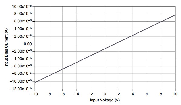
Input bias current
A consequence of having a finite input impedance is that the module requires a small amount of current to be able to detect a signal. Theoretically, this value should be 0 A, but in practice, this is not possible. Take the specified value into consideration when reading the measurement.
Example
NI 9224 has input bias current of 6 uA at an input voltage of +8 V. The input bias current flowing through the source impedance creates an error voltage. For example, if the measured source using the NI 9224 has an output impedance of 1 kΩ, the reading of the module would be 8.006 V, which includes the error voltage of +6 mV.
See Also
Input coupling
Some modules such as the NI 9234 and NI 9250 support both DC and AC coupled modes. When DC coupling mode is selected, any DC offset in the source signal is passed on to the ADC. When AC coupling mode is selected, a high pass filter is enabled at the input of the signal path, filtering out most DC content of the signal.
Example
NI 9250 allows software-selectable input coupling between DC and AC coupling modes. The AC filter has 3 dB point at 0.43 Hz.
See Also
Input delay
Input delay is the total path delay from the input pins to the data being ready to be read. In some modules, the input delay is specified as a function of the sampling frequency, whereas in others it is specified as a value.
The input delay specification only applies to modules with a delta-sigma ADC. Adding modules with different input delays to a system may incur synchronization issues between those modules. This can be compensated with a filter that delays the signal from the module with the lower input delay to synchronize with the module that has the higher input delay.
Example
NI 9250 has an input delay is 34/fs + 2.7 µs. For example, when the sample rate is set to 102.4 kS/s, the input delay will be 334.73 µs.
NI 9224 specifies input delay for each timing mode. For example in High Resolution the input delay is specified at 199.290 ms.
Note: Some C Series Modules list their input delay in mixed fraction notation. The NI 9239 is an example of this. Its input delay is (40+5/512)/fs + 3.3µs.
See Also
How Can I Compensate for Different Group Delays with C Series Modules in LabVIEW FPGA?
Input impedance (Analog)
Input impedance is a measure of how the input circuitry on the module impedes current from flowing through to analog input ground. For an ideal ADC, this value should be infinite, meaning no current will flow from the input to ground. However, in practice this is not possible. The implication of some finite input impedance is that the ADC will have some degree of loading down a circuit, particularly those of high output impedance. It is typical for sensors to have low output impedance.
Example
The NI 9220 has an input impedance of Zin >1 GΩ. Taking worst case scenario of lowest input impedance, the single ended measurement can be viewed as the following simplified circuit, assuming a sensor with output impedance
Zout = 150 Ω.
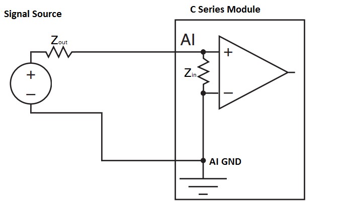
The series combination of the sensor output impedance and the module input impedance introduces measurement error. For example if the signal source is at 5 V, the actual signal measured by the module will be:
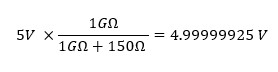
Thus, there will be a measurement error of 750 nV. This will be negligible when using the NI 9220 since the error is much smaller compared to the module's gain error. However, if the source impedance is for example, 10 MΩ then the error will be 50 mV. Thus, it is important to have an idea of the source impedance as well as the module input impedance so that the measurement error from these two sources can be known.
See Also
Input range
For analog input, this is the maximum positive and negative value that can be measured with accuracy. Some modules have multiple user-selectable input ranges that can be used to provide a higher resolution and improved accuracy at lower level signals.
Example
The NI 9224 specifies a typical input range of ±10.54 V. This is the maximum voltage that a typical module is able to measure accurately.
The NI 9224 also specifies a minimum input range of ±10.4 V. This is maximum voltage that every single unit of NI 9224 is warranted to measure accurately.
See Also
Differences Between Accuracy, Code Width and Bits of Resolution
Instantaneous Measuring Range
The Instantaneous Measuring Range is the actual input range that the module can read accurately. Typically this specification is accompanied by an operating input rating because these modules are intended to be used with sinusoidal input signals that will have an RMS Current. The operating input rating is the maximum RMS current that can be accurately measured by the module continuously. Both specifications need to be adhered to in order to guarantee accurate measurements.
Example
The NI 9246 has an Instantaneous Measuring Range of at least +/-30.6A so it can accurately measure current values up to +/-30.6A, but those signals also must have an RMS current of less than +/-22Arms.
See Also
Maximum working voltage, or Common mode voltage range
Maximum working voltage specifies the total voltage level that a module can tolerate on any analog input channel before data validity on other channels becomes an issue. The combination of the signal to be measured and any common mode voltage with respect to AI GND should not exceed this maximum working voltage specification to guarantee accuracy on other channels. Note that the maximum working voltage is independent of the input range of the module.
Example
A 10 V peak sine wave with 2.5 VDC common mode is being measured on NI 9205, which has a maximum working voltage of ±10.4 V as shown below:
The combination of the two signal peaks at +12.5 V, which exceeds the maximum working voltage. Exceeding the maximum working voltage puts the data validity on other multiplexed channels at risk due to excess charge on the multiplexer not having enough time to settle.
See Also
Normal-mode rejection ratio (NMRR), or Noise rejection
NMRR is the rejection that the analog front end provides at a particular frequency. It is specified in decibels (dB) and is usually at powerline frequencies, such as 50/60 Hz.
Example
The NI 9212 specifies noise rejection of 74 dB at 50/60 Hz when the module is used in high resolution mode. If there is a 50 Hz power line signal of 100 µVrms that is coupled on the signal path, this will be rejected to 20 nVrms by the NI 9212.
See Also
Noise, Idle channel noise, Input noise, or Root mean square (RMS) noise
Additional system noise generated by the analog front end, measured by grounding the input channel. The specified value is the RMS noise in Volts RMS or in LSB RMS. The noise measurement is done by taking a large number of samples and obtaining the standard deviation of the samples. Since the idle channel noise most likely has a Gaussian distribution with a mean of zero, the RMS noise is equivalent to one standard deviation. Thus, about 66% of the samples taken by the module will have noise values that fall within the RMS noise value. Noise specification is the effective resolution of the device since anything lower than the noise value would not be able to be perceived.
Example
NI 9223 specifies 0.75 LSB rms noise. NI 9223 has an input range of ±10 V with 16 bits of resolution, thus the value of 1 LSB in volts is 305 µV and the noise value is then 0.75 x 305 µV which is 229 µVrms.
See Also
Oversample rate
This terminology applies only to modules with delta-sigma ADCs. Delta-sigma ADCs use sample rates that are large multiples, such as 128 times the Nyquist rate of a given signal, for instance. For example, to sample a 25 kHz signal, a sample rate greater than the Nyquist rate (above 50 kHz) would be sufficient. However, a delta-sigma ADC using an oversample rate of 128 will sample the signal at a much higher frequency than the Nyquist rate. This approach has several benefits, such as better anti-aliasing and higher resolution.
The oversampled data is processed by a digital filter within the ADC before the data is made available as an output. Since it takes a non-zero amount of time for the oversampled data to be processed by the digital filter, the output data rate is always lower than the oversample rate. The output data rate equals to the oversample rate divided by the ADC decimation ratio.
Example
The NI 9218 has an oversample rate of 64*fs, where fs is the software-selected output data rate.
The NI 9250 has an oversample rate (1024*fs, 512*fs, 256*fs, 128*fs, 64*fs, or 32*fs) that is dependent on the software-selected output data rate.
See Also
Oversample rate rejection, or Alias rejection
Alias rejection specifies how much rejection is provided at a given frequency that will alias back into the module’s passband. To understand alias rejection, first the aliasing property of a sampled system has to be understood. The Nyquist theorem states that the frequency of a signal with frequency f can be accurately measured as long as it is sampled at greater than 2f. If an attempt is made to measure frequencies above f by sampling the signal at 2f, an alias or false images of the signal will be created at frequencies below f. These false frequencies will appear as mirror images of the original frequency around the Nyquist frequency.
where
R (sampling rate) =100MS/s
fs (signal being sampled) =70MHz
fN (the Nyquist frequency, with respect to sampling rate R) = 50MHz
fa (aliased frequency) =30 MHz
The frequency of the aliased signal can be found from the following equation:
fa = |R*n-fs|
where n is the closest integer multiple of the sampling rate (R) to the signal being aliased.
The oversample rate rejection when specified at the minimum software-selected output rate also provide guidance on the amount of rejection provided by the device on signals that may appear in alias holes due to the digital filter.
Example
NI 9250 specifies alias rejection, at oversample rate, as 100 dB at 3.2768 MHz for data rate, fs = 102.4 kS/s. Since the data rate is an integer multiple of the oversampling rate, a signal at the oversample rate will alias back between 0 Hz and 51.2 kHz, which is the Nyquist band. With 100 dB of rejection, this signal will be attenuated by 100,000x.
See Also
Aliasing and Sampling at Frequencies Above the Nyquist Frequency
Low Frequency Alias Rejection with NI Dynamic Signal Acquisition Modules
Overvoltage protection, overvoltage withstand, or safe operating area (SOA)
The amount of voltage module can withstand between input pins for a specified duration before it becomes damaged.
Example
The NI 9223 has ±30 V overvoltage protection on each channel. The module can withstand a maximum voltage difference of 30 V between pins continuously without sustaining damage.
The NI 9244 has overvoltage withstand specified at 1000 Vrms for 1 second, and 800 Vrms continuous.Thus, if a 1000 Vrms signal was applied to the module is warranted to only withstand this up to 1 second before it gets damaged. If a 800 Vrms voltage is applied to the module then the module is warranted to withstand this continuously.
For some modules the overvoltage withstand is a function of the signal frequency.The chart below shows the SOA for the NI 9775. The orange trace indicates the protection limit of the module as a function of input voltage and input signal frequency. For example, if the input signal frequency is 5 MHz, the module is protected up to 30 Vpk. However, if the signal frequency is 25 MHz, the module is only protected up to 10 Vpk.
See Also
Channel-to-channel phase mismatch
Channel-to-channel phase mismatch defines the difference in phase on any given channel relative to a reference channel. It is specified as a function of the input frequency.
Example
NI 9250 specifies channel-to-channel gain mismatch of fin * 0.035° maximum, where fin is in kHz. For example, if the input signal frequency is 2 kHz, the maximum difference in phase on one channel relative to any other channel on the module. is 0.07°.
Sample rate
Sample rate specifies how often an ADC converts data from analog to digital values. Some modules have only one ADC, so the sample rate is shared or multiplexed across channels. This is also known as having a scanned sampling mode. While other modules have a dedicated ADC per channel, also known as simultaneous sampling mode. Sample rate is measured in Samples per second (S/s) or Samples per second per channel (S/s/ch) when acquiring from multiple channels.
Example
NI 9205 specifies sampling rate of 250 kS/s aggregate. NI 9205 is a multiplexed module,it only has a single ADC, thus if it is configured to acquire on all of its 16 differential channels, the maximum sample rate on each channel will be 15.625 kS/s (250/16).
NI 9223 specifies a sampling rate of 1MS/s/ch. NI 9223 is a simultaneous input module with each channel having an independent ADC so the sample rate on each channel is 1 MS/s.
Surge withstand
The amount of sudden voltage the module can withstand for a specified duration before it gets damaged.
Example
NI 9244 specifies a surge withstand voltage of 8 kV (1.2 µs / 50 µs). The module was tested with a surge voltage waveform as the one shown below. Where Um is 8 kV.
See Also
Transducer electronic data sheet (TEDS)
TEDS is an IEEE1451.4 standard for sensors that provide critical attributes for modules to properly use signals from an analog sensor.
Example
The NI 9250 supports IEEE 1451.4 TEDS Class 1.
See Also
Analog Output
Capacity drive
How much capacitance the module is able to drive before the accuracy specifications of the modules are exceeded. Exceeding this value no longer guarantees that the integrity of the output signal matches the specification.
Example
The NI 9264 has a capacity drive specification of 1,500 pF maximum.
Current drive (for voltage)
The maximum amount of current that a module can output, which also defines the amount of load impedance the module is able to drive while still maintaining the full output range. It is typically specified across each channel and as a maximum per module. Exceeding this specification interferes with the module's ability to maintain full output range but does not damage the module as the module provides short-circuit protection. NI chassis do support modules at maximum current drive in all slots simultaneously.
Example
The NI 9264 has the following current drive specification:
If the module is configured to produce an output on one channel, then the current drive of that one channel is ±4 mA. Another way of looking at it is that in order to output ±10 V on one channel, the load resistance has to be at least
10 V / 4 mA = 2.5 kΩ.
However, if the module is configured to output on multiple channels, then the total current the module is able to drive is limited to ±16 mA. For example, if the module is configured to output a voltage on four channels and the load on each of the four channels is ± 4mA , the module will able to do this since the maximum current of ±16 mA is yet to be exceeded. However, if it were five channels instead of four, then the module is no longer warranted to drive ±4 mA per channel since the total current drive of the module has exceeded ±16 mA.
Differential Non-Linearity (DNL) / Integral Non-Linearity (INL)
DNL is the difference between the ideal step size of a digital-to-analog converter (DAC) and the actual value that is output, typically measured in LSB. In an ideal DAC, the DNL value would be 0 LSB. INL is the compound effect of DNL so the INL specification is often used in accuracy calculations.
Example
The NI 9264 has DNL specified at ±1 LSB maximum, and INL specified at ±12 LSB maximum. This means that for any value that is output from the DAC, the actual value can be ±1 LSB away from the value programmed. For example, if the user programs the DAC to output a value of 1 V, the output (not including effects of accuracy) can range from:
See Also
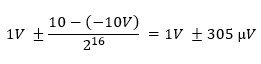
Digital-to-analog converter (DAC) resolution
The number of bits that represents an analog signal when converting from a digital value.
Example
The NI 9264 has a DAC resolution of 16 bits, which means there are 2^16 or 65,536 discrete values that can be output within the output range of ±10 V, with each step being 10 V / 65,536 = 305 µV.
See Also
Generating a Signal: Types of Function Generators, DAC Considerations, and Other Common Terminology
Monotonicity
Monotonicity is the guarantee that when DAC codes increase, the output voltage also increases. A module is warranted to be monotonic if the DNL is no greater than ±1 LSB.
Example
NI 9264 has a DNL of ±1 LSB maximum which implies that the monotonicity of the module is guaranteed. It also specifies monotonicity of 16 bits which implies that the transition between all 16 bits are monotonic.
See Also
Maximum load, Maximum resistance load for current
Defines the maximum load a current output module can drive for a given load resistance before it reaches the output compliance voltage.
Example
The NI 9265 has a maximum load of 600 Ω for output current at 20 mA, because the compliance voltage of the module is 12 VDC. It is the compliance voltage and the output current that define the maximum load drive for the module. For example, if the desired output current is only 10 mA then the module could drive loads up to 12 V / 10 mA = 1.2 kΩ instead.
See Also
Output impedance
Output impedance is the impedance that is effectively in series with an analog output channel, as illustrated below:
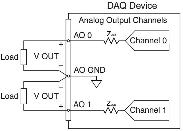
A low output impedance allows more of the voltage generated to be dropped across the load of the analog output. It is important to take the output impedance into account to ensure that the desired accuracy in voltage is achieved.
Example
The NI 9264 has an output impedance of 2 Ω. This means that if a load connected has an impedance of 500 Ω, and the voltage specified by the user is 1 V, then the actual voltage on the load would be 0.996 V, or 4 mV, less than expected. At this voltage, there will also be 1.99 mA drawn from the module.
Output range
The maximum positive and negative values that can be generated by the module. Some modules have multiple output ranges that can be used to provide a higher resolution at lower level signals.
Example
The NI 9265 is a current output module with an output range of 0 mA to 20 mA.
The NI 9264 is a voltage output module with an output range of ±10 V.
See Also
Maximum load, maximum resistance load for current
Differences Between Accuracy, Code Width and Bits of Resolution
Settling time
The amount of time it takes for an analog output value to stabilize to within a certain degree of precision. Settling time is related to load capacitance. A lower load capacitance value may lead to a shorter settling time.
Example
The NI 9264 specifies settling time as:
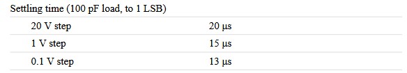
Here the settling time applies to 100 pF of load capacitance and the stated time is how long it takes the output to settle to within 1 LSB. So for a 20 V step size, with output driven from -10 V to 10 V, it takes 20 µs to settle to 9.999695 V. It takes less time to settle in the case of a 1 V step size or a 0.1 V step size.
Slew rate
Slew rate specifies the rate of change for the analog output channels in a given module. It is typically measured in V/µs. Settling time for output is calculated with slew time already included in the calculation. It is important to consider slew rate when designing a system for high amplitude high frequency signals, as the large swing in amplitude may exceed the slew rate for a given module.
Example
The NI 9264 has a rate of 4 V/µs, this means that the highest theoretical frequency that can be generated if the output toggles between -10 V and 10 V is 200 kHz. However, we know that it is not possible to generate a 200 kHz signal since the limitation here is the output data rate of the module that is only 25 kS/s. Here the slew rate can be seen as a limitation of the signal edge rated instead of a limitation of the output frequency.
See Also
Update rate
For analog output, update rate specifies how often in time the module produces an output. Most NI C Series modules have a single DAC per analog output channel, but will all share the FIFO where the analog output data is stored. The rate at which data can be read from this FIFO and transferred to the different DACs on board can sometimes limit the update rate when using multiple AO channels on the same module. Update rate is measured in samples per second (S/s) when output from a single channel, or samples per second per channel (S/s/ch) when output from multiple channels.
Example
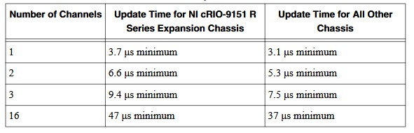
Based on the specifications for NI 9264, it takes the module 3.1 µs minimum to update its output when it is configured to output on just 1 channel. It takes longer if it is configured to output on multiple channels.
Analog General
Accuracy gain and offset
Accuracy refers to how close to the correct value of a measurement is. Absolute Accuracy at Full Scale is a calculated theoretical accuracy assuming the value being measured is the maximum voltage supported in a given range. The accuracy of a measurement will change as the measurement changes, so to be able to make a comparison between modules, the accuracy at full scale is used. Note that absolute accuracy at full scale makes assumptions about environment variables, such as 25 °C operating temperature, that may be different in practice.
- Nominal Range Positive Full Scale—The ideal maximum positive value that can be measured in a particular range
- Nominal Range Negative Full Scale—The ideal maximum negative value that can be measured in a particular range
- Calibrated Gain Error—Gain error inherent to the instrumentation amplifier and is known to exist after a self-calibration
- Gain Tempco—The temperature coefficient that describes how temperature impacts the gain of the amplifier compared to the temperature at last self-calibration
- Calibrated Offset Error—Offset error inherent to the instrumentation amplifier and is known to exist after a self-calibration
- INL Error (relative accuracy resolution)—The maximum deviation from the voltage output of an ADC to the ideal output. Can be thought of as worst case DNL.
- Offset Tempco—The temperature coefficient that describes how temperature affects the offset in an ADC conversion compared to the temperature at last self-calibration
Example
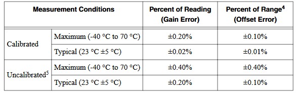
NI 9223 publishes the table above under the accuracy section. For example, when the module is configured to return calibrated data and 5 VDC is being measured, the maximum expected gain error for the full operating temperature range is ±0.20% x 5 V = ±10 mV. The offset error is ±0.10% x 10 V = ±10 mV, so the total uncertainty when measuring a 5 V signal will be 5 V ±20 mV.
See Also
Crosstalk
The measure of how much a signal on one channel can couple onto, or affect, an adjacent channel. Crosstalk exists any time an amplitude-varying signal is present on a wire or PCB trace that is physically close to another wire or PCB trace. Crosstalk is also sometimes referred to as seeing ghosting, floating or other unexpected voltages.
Example
The NI 9224 has a crosstalk specification of -125 dB at an input frequency of 1 kHz. For example, if AI 0 is driven with a 10 Vpk, 1 KHz input signal, a 5.6 µVpk 1 kHz signal will be coupled onto AI 1.
See Also
Troubleshooting Unexpected Voltages, Floating, or Crosstalk on Analog Input Channels
Spurious free dynamic range (SFDR)
SFDR is the usable dynamic range before spurious noise interferes with or distorts the fundamental signal. The amplitude of the fundamental signal is usually -1 dBFs. SFDR is the measure if the ratio in amplitude between the fundamental and the largest harmonically or non-harmonically related spur from DC to the full Nyquist bandwidth (half the sample rate). A spur in any frequency bin on spectrum analyzer, or from a Fourier transform, of the analog signal expressed in dBc.
The following figure illustrates how SFDR is measured.
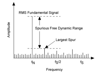
Example
The NI 9250 specifies its non-harmonic SFDR of 138 dBFs.
See Also
IEPE excitation current
This is the excitation current that the module is capable of providing to IEPE sensors. It can be turned on or off in software.
Example
NI 9232 specifies a typical excitation current of 4.25 mA.
IEPE excitation voltage
This is the voltage drop that the IEPE circuitry can handle while maintaining its constant current supply.
Example
The NI 9232 specifies the IEPE excitation voltage (in terms of a compliance voltage) of 22 V minimum which can be enabled or disabled through software.
See Also
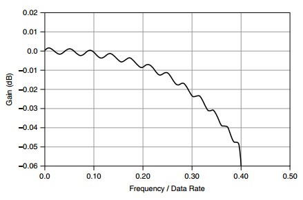
Flatness
The signals within a passband have frequency-dependent gain or attenuation. The small amount of variation in gain with respect to a reference frequency is called the passband flatness.
Example
NI 9250 specifies flatness of 0.03 dB maximum, from DC to 20 kHz. This means that the maximum variation between any signal at DC and 20 kHz is at most 0.03 dB.
See Also
Channel-to-channel phase mismatch
Channel-to-channel phase mismatch defines the difference in phase on any given channel relative to a reference channel. It is specified as a function of the input frequency.
Example
NI 9250 specifies channel-to-channel gain mismatch of fin * 0.035° maximum, where fin is in kHz. For example, if the input signal frequency is 2 kHz, the maximum difference in phase on one channel relative to any other channel is 0.07°.
Intermodulation distortion (IMD)
IMD is another measure of distortion due to non-linearity in the module. IMD is often used to measure the distortion of a module near the high-frequency limit of the module or the measurement system. If the input to the module is a multi-tone signal, the non-linearity present in the module would cause the tones to mix and create new tones in the spectrum which are undesirable. The level of these new signals are defined by IMD.
Example
NI 9250 specifies intermodulation distortion that is tested according two standards. -101 dB (SMTPE 60 Hz + 7 kHz) and -103 dB (CCIF 14 kHz + 15 kHz).
See Also
Input bandwidth
The input bandwidth, often also specified as the -3 dB bandwidth, is the frequency at which the magnitude of the signal is 3 dB below the magnitude of the signal at DC. The -3dB is the industry standard is specifying the input bandwidth of the product.
Example
NI 9224 specifies input bandwidth of 1.3 kHz. If the input to the module was a 1 VDC signal, the module would measure 1 VDC. If the input to the module was a 1 Vpk signal with a frequency of 1.3 kHz, the magnitude of the signal will be 0.707 Vpk.
See Also
LSB weight, or Scaling coefficient
This is a scaling coefficient that when multiplied with the ADC output, which is in codes, gives the engineering units. Knowing this scaling is only important when reading in raw ADC codes otherwise this can be ignored since the scaling from codes to engineering units occurs when reading in calibrated mode.
Example
The NI 9244 specifies a scaling coefficient of 118,911 nV/LSB. This relates to the specified full-scale input in voltage of 997.5 Vpk. When an NI 9244 is driven with a positive full-scale input, the ADC code will be 8,388,608 which is 2^23; the ADC code is raised to the power of 23 here instead of 24 because the module carries out internal software manipulation to use the one of the 24 bits as a sign bit. Thus, 8,388,608 x 118,911 nV/LSB = 997.5 Vpk ; likewise when the input is at negative full-scale, the ADC code will be -8,388,608 x 118,911 nV/LSB = -997.5 Vpk
Gain and offset drift
Gain and offset drift define how much can gain and offset errors change as a function of temperature. It is often specified as change per degree Celsius.
Example
NI 9224 has a gain drift of ±17 ppm/°C and an offset drift of 21 µV/°C. This means for a typical board the gain error changes by 17 ppm for every degree Celsius and the offset error by 21 µV for every degree Celsius. The gain drift is only applicable to the typical specification and outside the ±5 °C window.
See Also
Phase non-linearity
Ideally in a linear phase system, the phase and the frequency of the signal have a linear relationship. This means that input signals of all frequencies have the same time delay through the system. Phase non-linearity is an expression of the extent to which the phase-frequency function deviates from the ideal.
Example
NI 9239 specifies phase non-linearity of 0.11° maximum. This means that the maximum deviation that can be expected from the ideal linear frequency-phase curve is 0.11°.
Total harmonic distortion (THD)
In an ideal system, the Fast Fourier Transform (FFT) of a sinusoid results in a single peak at a specific frequency. However, in real world systems, the presence of non-linearity and noise result in imperfections. When a signal of particular frequency, f1 passes through a nonlinear system, the output consists of f1 and its harmonics.
Harmonic distortion is the measure of the power contained in the harmonics of the signal relative to the power in the fundamental. Total harmonic distortion (THD) is a measure of the power summation of all the harmonics in the spectrum relative to the power in the fundamental. It can be defined as power ratio or percentage ratio.
When expressed in power ratio:
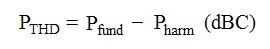
Where PTHD is the power of the total harmonic distortion, Pfund is the fundamental signal power in dB, and Pharm is the total power of the harmonics in dB.
When expressed in percentage ratio:
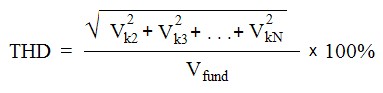
Where VkN is the amplitude of the Nth harmonic, Vfund is the fundamental signal amplitude.
Example
NI 9223 specifies THD of -85 dB with a 20 Vpp signal at 1 KHz being the test signal. This means that the difference in power between the fundamental tone at 1kHz and the sum of all the harmonics is equivalent to -85 dB.
See Also
Thermocouple Subsystem Specifications
Cold-junction compensation (CJC) sensor accuracy
The thermocouple itself relies on the principle that an electrical potential exists at the junction of two different metals. CJC becomes necessary because the junction between each end of the thermocouple and your measuring system (connector block, terminal block) also adds a potential difference to the thermocouple voltage. This is compensated by using an onboard CJC sensor to measure the temperature between the thermocouple and the measuring system. CJC sensor accuracy is the accuracy specification of the CJC sensor only.
Example
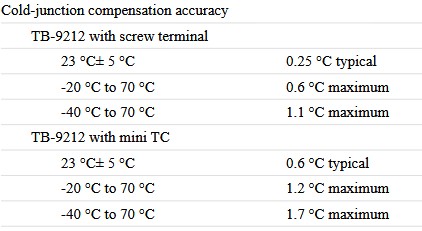
The NI 9212 specifies CJC accuracy for both types of supported connectors. The CJC accuracy is taken into account in the published total accuracy of the thermocouple, such as table 1 in the NI 9212 datasheet.
See Also
What is CJC and Why Does My Data Acquisition Board or Signal Conditioning Unit Include a CJC Sensor?
Input open thermocouple detection (OTD) bias current, or Open thermocouple detection (OTD) input current
Open thermocouple detection (OTD) circuitry is used to detect thermocouple damage or thermocouple errors. The OTD circuit detects thermocouples that may have an open junction when connected to the measurement device, by injecting current into the thermocouple and reading the voltage back. In the case where the thermocouple junction is open, a significantly high voltage value is returned. The current that in injected into the thermocouple is the input OTD bias current. In some systems, the OTD status can be polled programmatically to help prevent unexpected readings.
Example
NI 9212 specifies an input OTD bias current of 37.4 nA at 23 °C ±5 °C. For example, if the source impedance of the thermocouple is 0.5 Ω, then an additional error of 18.7 nV can be expected from the OTD bias current.
See Also
Input open thermocouple detection (OTD) bias current drift
Open thermocouple detection (OTD) circuitry is used to detect thermocouple damage or thermocouple errors. Input OTD bias current drift defines how much the input OTD bias current drift changes as a function of temperature. It is often specified as change per degree Celsius.
Example
The NI 9212 has an input OTD bias current drift specified at ±12 pA/°C maximum. This value is normalized to 23 °C
For example if the source impedance of the thermocouple is 0.5 Ω, and operating ambient temperature of the module is 43 °C, then an additional error of 20 x ±12 pA/°C x 0.5 Ω = 120 pV can be expected.
See Also
Offset error from source impedance with open thermocouple detection (OTD)
Open thermocouple detection (OTD) circuitry is used to detect thermocouple damage or thermocouple errors. The offset error from source impedance with OTD is the input OTD bias current normalized to 1 Ω.
Example
When the offset error from source impedance with OTD is add 37.4 nV per Ω at 23 °C ± 5 °C. For example if the source impedance of the thermocouple is 0.5 Ω, then an additional error of 18.7 nV can be expected from the OTD bias current.
See Also
Open thermocouple settling time when switching OTD on/off
Open thermocouple detection (OTD) circuitry is used to detect thermocouple damage or thermocouple errors. In modules like the NI 9214 it is possible to toggle the OTD settings on and off through software.
Open thermocouple settling time when switching OTD on/off is the amount of time recommended to wait after enabling or disabling the OTD circuit before taking temperature measurements.
Example
The NI 9214 specifies an open thermocouple settling time of 6 seconds before it is recommended to take a temperature measurement after switching OTD on or off.
See Also
Open thermocouple settling time
Open thermocouple detection (OTD) circuitry is used to detect thermocouple damage or thermocouple errors. OTD settling time is the amount of time required by the module before the open thermocouple is detected.
In most modules this number is so small that it is not specified, however, the value is specified in cases when the number is more significant.
Example
NI 9212 has an open thermocouple settling time of 0.75 seconds. If a thermocouple is open, it would take 0.75 seconds before the module detects it.
See Also
Measurement sensitivity
Measurement sensitivity represents the smallest change in temperature that a measurement sensor can detect. It applies to thermocouples and the exact value is dependent on the thermocouple type. This is similar to the LSB weight specification where the smallest change in voltage that can be detected by a voltage input module.
Example
NI 9212 specifies measurement sensitivity of 0.05 °C for type J, K, T, and E thermocouples when the module is operated in the high speed mode. This means the smallest change in temperature that can be detected when using these thermocouple types is 0.05 °C.
See Also
Temperature measurement range
This range specifies the highest and lowest temperatures that can be measured with warranted accuracy by the module.
Example
The NI 9214 has a temperature measurement range specified to cover the entire temperature ranges defined by the National Institute of Standards and Technology (NIST) for all supported thermocouple types (J, K, T, E N, B, R, S). For example, the NI 9214 could measure across the Type K's temperature range: -270 °C to 1260 °C.
See Also
Thermocouple Types Definitions and Temperature Ranges - NIST
Thermocouple types
Defines the type of thermocouple that can be used with the module. Thermocouple types are standardized and identified by letter type, with each type made up of a particular chemical composition and each suited to measure within a particular temperature range.
Example
The NI 9212 can be used with thermocouples types J, K, T, E, N, R, S, and B.
See Also
Thermocouple Types Definitions and Temperature Ranges - NIST
Digital Subsystem Specifications
Digital Input
Input current, Input high current (IIH), or Input low current (IIL)
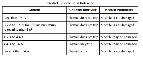
Ideally, the input impedance of a device is infinite and no current will be drawn, however, this is not achievable in practice. When reading in a digital value at either 0 V or 5 V, a small amount of current will be drawn by the digital input circuitry of the NI device. The amount of current drawn while measuring a high voltage level is input high current, likewise, the amount of current drawn while measuring a low voltage level is input low current. It is important to ensure that a digital signal being measured has the capability to tolerate the current values specified. Depending on the module, this specification may be listed as input current, IIH, IIL, or under digital logic levels as sinking and/or sourcing current.
Example
The NI 9403 will either sink or source up to 250 µA when 0 V ≤Vin ≤ 5 V. The NI 9402 will either source up to 55 µA when Vin = 0 V or sink up to 150 µA when Vin = 4.5 V.
The NI 9426 will either source up to 150 µA when in the OFF state or sink at least 330 µA when in the ON state. This applies to all digital lines.
See Also
Input impedance, or Input resistance
Input high voltage (VIH), or Input low voltage (VIL), or Input voltage
Input capacitance
Input capacitance can be used to determine input impedance when an NI module’s input circuitry involves more than a typical pull-down resistor. Input impedance is needed to determine the amount of current needed to drive an input of a module and can be calculated by the following formula:
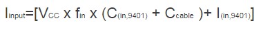
Where:
Vcc is the voltage provided by the user's circuit that is driving the NI 9401
fin is the frequency of the voltage provided by the user's circuit that is driving the NI 9401
C(in,9401) is the input capacitance specified in the manual
Ccable is the capacitance of the cable used
I(in,9401) is the input current of the NI 9401
Example
The NI 9401 specifies an input capacitance of 30 pF. Since the NI 9401 provides a DIO TTL signal type, impedance typically does not impact these types of applications. Instead, the current drive is the driving specification which can be calculated using the formula above.
For example, when providing a 2.2 V signal at 10 kHz, the necessary current needed to drive the input is Iinput=[2.2 V x 500 kHz x (30 pF + 1000 pF)+ 250mA] = 251.133 mA.
See Also
What is the Impedance of the NI 9401?
Input impedance, or Input resistance
Input impedance is a measure of how the input circuitry impedes current from flowing through to the digital input COM. Some modules separate this specification into input resistance and input capacitance. These modules do not have a linear I/V curve characteristic and can subsequently have a single resistance value for all voltages. Since impedance is a strong function of voltage, some modules do not specify input impedance but do provide expected currents at a given voltage.
Example
The NI 9402 specifies an input resistance of at least 49 kΩ minimum.
Meanwhile, the NI 9426 specifies an input impedance of 30 kΩ with a tolerance of ±5%. The series combination of the sensor output and the NI module input means that the voltage will be divided between the two impedance values, with the larger impedance bearing most of the voltage. This means that the voltage measured by the NI module is the output voltage of the sensor multiplied by the ratio of the input impedance to the sum of the NI module input and the sensor output impedance. For this example, the sensor output impedance will be 150 Ω.
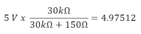
To illustrate an example of when input impedance becomes an important specification, take the hypothetical case where a sensor has an extremely high output impedance, such as 20 kΩ. Connecting the NI module to a sensor with this extremely high output impedance causes a 5 V nominal output from the sensor to be read as 3.00 V.
See Also
Input rise time, Input fall time, or Input rise/fall time
In theory, when a digital signal transitions from a low to high, it would happen instantaneously. However, it takes time for a signal to change between high and low levels. Rise time is the time it takes for a signal to rise from 10% to 90% of the voltage between the low level and high level. Fall time is the time it takes a signal to fall from 90% to 10% of the voltage between the low level and high level.
Example
The NI 9401 specifies an input rise/fall time of 500 ns maximum. This means that when reading a signal that is transitioning from TTL low to a TTL high, it can take up to 500 ns to transition from 0.525 V to 4.725 V.
Setup time
Setup time is the amount of time input signals must be stable before the module clocks the reading from the NI module and an accurate measurement value can be obtained. If the input signals do not remain stable, or within the upper and lower bounds of the specified voltage thresholds, during this time period then incorrect data may be measured.
Example
The NI 9403 specifies a setup time of 10 ns minimum. This means that an input high signal must remain between 2.2 V and 5.25 V for at least 10 ns before initiating a read for the NI 9403 to be able to accurately measure the digital logic level. Since the NI 9403 also has a hold time of 60 ns, the signal must remain stable for at least 70 ns.
See Also
Hold time
Hold time is the amount of time input signals must be stable after initiating a read from the NI module. If the input signals do not remain stable, or within the upper and lower bounds of the specified voltage thresholds, during this time period then incorrect data may be measured.
Example
The NI 9403 specifies a hold time of 60 ns minimum. This means that a signal must remain stable for at least 60 ns after initiating a read for the NI 9403 to be able to accurately measure the digital logic level. Since the NI 9403 also has a setup time of 10 ns, the signal must remain stable for at least 70 ns.
See Also
Hysteresis
Hysteresis defines the current and voltage level change that must occur for the NI module to recognize a transition. In this case, the transition observed is from the high to indeterminate state, and low to indeterminate state. This specification illustrates how much the voltage level can change below the ON state voltage level or above the OFF state voltage level before entering the indeterminate state again. The current component of the hysteresis specification defines a similar behavior for the specified current level.
Example
The NI 9425 specifies a hysteresis of at least 2 V. This means that if a signal transitions from 6 V to 4.5 V (i.e. a 1.5 V change), it will still be in an indeterminate state even though the logic level itself transitioned from indeterminate to the OFF state. If the signal transitions from 6 V to 4 V (i.e. a 2 V change), it will transition into the OFF state. The 60 µA current minimum specifies that the input current, which directly correlates with the input voltage, must be met.
See Also
Input high voltage (VIH), or Input low voltage (VIL), or Input voltage
Input delay time
Input delay time is the amount of time that the signal takes to propagate from the input pin of the module to the chassis or controller connection of the 15 pin DSUB. With respect to the input voltage, the input delay time is the time that the voltage across a channel must remain at the ON or OFF level to change the channel from ON to OFF, or from OFF to ON. This specification should also be considered when determining signal rates for an application as the input delay time may take longer than the allowed signal transition time.
Example
The NI 9411 specifies an input delay time of 500 ns maximum. Therefore, it takes 500 ns for the signal to propagate. This means that a signal must remain stable for at least 500 ns to be able to accurately measure the digital logic level.
See Also
Digital Output
Power-on output state
Power-on output state specifies the default state (ON or OFF) of the output channels when the NI module is powered on.
Example
The NI 9476 power-on output state is “channels off”. This means that the output channels default to be in the OFF state upon power-on.
See Also
Understanding Power-On and Startup Output States for CompactRIO Output Modules (FPGA Interface)
Output high voltage (VOH), or Output low voltage (VOL), or Output voltage
The operating voltage ranges that can be expected from an output signal when generating a logic high or logic low. The output voltage generally also specifies the amount of current that the module can sink and maintain the high or low output voltage.
Example
The NI 9402 specifies that the maximum voltage output is 3.4 V for a high voltage. For a low voltage, the VOL specifies that the module can sink 2 mA and output a maximum of 0.3 V.
See Also
Output delay time
Output delay time is the amount of time that the voltage across a channel takes to change the channel from ON to OFF, or from OFF to ON. This time also includes the propagation time from the chassis connection to the module output pin. This specification is defined at full load with the maximum current drive and voltage output range. This specification should also be considered when determining signal update rates for an application as the output delay time may take longer than the allowed signal transition time.
Example
The NI 9472 specifies an output delay time of 100 µs maximum at full load. This means that a signal can take up to 100 µs maximum to propagate to the front end of the module when using a voltage range of 30 V at the maximum continuous output current 0.75 A.
See Also
Continuous output current per channel
Continuous output current is the amount of current each channel can source without moving outside the bounds of the specified operating conditions; this may include module shutdown or damage. See your specific module's datasheet to determine your module's behavior.
Example
The NI 9472 specifies a continuous output current per channel of 0.75 A. The NI 9472 specifies the following behavior when more than 0.75 A per channel is sourced:
Switched output current per channel
Switched output current is the amount of current each channel can source at a specified output frequency, maximum duty cycle, and 2 meters of cabling. This specification applies to the NI 9478.
Example
The NI 9478 specifies a switched output current on one channel of 4 A maximum with an output frequency of 10 kHz. When outputting at a higher frequency of 20 kHz with one channel on, the maximum is 3.33 A.
Output resistance
Output resistance is the resistance component to an NI module’s input impedance. In the figure below, the output impedance is 50 Ω. Matching characteristics impedance improves signal loss and reflections.
Example
The NI 9402 specifies an output resistance of at least 49 Ω minimum. This allows for the characteristic impedance of the BNC cable to be matched to 50 Ω to ensure optimal signal integrity.
See Also
Output impedance
Output impedance (R0) is the impedance that is effectively in series with a digital output channel. A low output impedance allows more of the voltage generated to be dropped across the load. It is important to take the output impedance into consideration to ensure that the voltage level desired is achieved. The output impedance with output current can be used to determine the expected output voltage.
Example
The NI 9475 specifies an output impedance of 0.14 Ω maximum. Using the following formula with a maximum continuous output current of 1 A and an external power supply of 60 VDC:
Vsup - (I0 x R0)
The minimum output voltage for this application can be calculated as 59.86 V.
See Also
Continuous output current per channel
Output high voltage (VOH), or Output low voltage (VOL), or Output voltage
Channel-to-channel skew
Channel-to-channel skew is the amount of time between the first output channel updating and the last output channel updating. It is the time delay between two channels that are intended to be updated at the same time. It is the time difference between a rising or falling edge on one channel relative to another when that rising or falling edge was read or output at the same time.
Example
The NI 9403 specifies channel-to-channel skew at 265 ns maximum which means there may be up to a 265 ns delay between two channels that are transitioned at the same time. There is no way to prevent skew on the output lines of this module. The NI 9401 is recommended for applications where tighter control over skew is required. The maximum channel-to-channel skew for the 9401 is 100 ns, equal to its maximum update rate.
Output voltage
Output voltage defines the range of voltage that the NI module can supply on its output lines. For these NI modules, the output voltage is defined in terms of the output impedance, the output current, and the external power supply voltage range.
Vsup - (I0 * R0)
Example
The NI 9476 has an output impedance of 0.3Ω maximum and a continuous output current of 200 mA maximum when using a 36 V DC supply voltage. Therefore, at full load, the maximum output voltage would be 35.94 V.
See Also
Output high current (IOH), or Output low current (IOL)
Module output current
The maximum guaranteed current that the module can drive from all the input/output lines without going into an overcurrent state.
Example
The NI 9403 specifies a module output current of 64 mA maximum. With 32 channels, that means each module can source up to 2 mA. If more current is drawn through the output channels, the module will go into an overcurrent state, during which the module will tri-state all of the DIO channels for approximately 280 ms. The module continues to remain in the overcurrent state until the overcurrent condition is removed.
See Also
Output high current (IOH), or Output low current (IOL)
External power supply voltage range
External power supply voltage range (Vsup or Vsup-to-COM) defines the accepted voltage range of the DC power supply.
Example
The NI 9476 defines an external power supply voltage range of 6 V DC to 36 V DC. Some NI modules, such as the NI 9411 provide this information under an External Power Supply section.
See Also
Vsup current consumption
The Vsup current consumption specifies the maximum amount of current that is required from the user’s external power supply.
Example
The NI 9476 defines a Vsup current consumption as 28 mA. This means that the external power supply used with the NI 9476 must be able to provide up to 28 mA of current.
See Also
Digital General
Digital power-on line direction
For modules that are bidirectional, the digital power-on line direction specifies whether the lines default as inputs or outputs when the module is powered on.
Example
The NI 9403 lines will default to input channels when powered on.
Maximum signal switching frequency, or Maximum I/O switching frequency
The switching frequency is how fast the module circuitry can update. This means that the module may miss a high-to-low or low-to-high transition if it occurs faster than the switching frequency. This specification is relevant for applications that use a CompactRIO chassis. Depending on the duty cycle and rates requested, faster designs may work but NI does not guarantee these limits and it would require a user to validate their final design. Switching frequency is specified per channel because it is directly related to the circuitry’s ability to update.
Example
The NI 9401 is capable of a 5 MHz switching frequency when using all 8 output channels. This means that all 8 channels can update their outputs every 0.2 µs.
See Also
Input/output type
Input/ output type is used to define what type of logic signals the NI module is compatible with, how the signal is terminated, and whether the lines sink or source current. Sinking and Sourcing are terms used to define the control of direct current flow in a load.
A sinking DIO provides a grounded connection to the load.
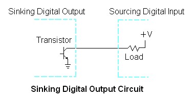
A sourcing DIO provides a voltage source to the load.
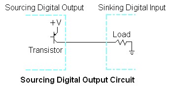
TTL (transistor-transistor-logic) and LVTTL (low voltage transistor-transistor logic) signals must meet defined specifications to be compatible with the standard. These NI modules are sinking/sourcing modules.
- TTL signals have a voltage range from 0 V to 5 V.
- LVTTL signals have a voltage range from 0 V to 3.3 V.
Differential and single-ended determine what type of signal the NI module can measure.
- Differential input digital lines measure differential signals such as differential encoders and LVDS signals.
- Single-ended digital lines cannot measure differential signals.
Example
The NI 9403 defines input/output type as TTL, single-ended. This means that this module is not compatible with differential signals but is able to measure/output TTL-compatible 5 V signals. As it is a TTL module, it has sinking inputs and sourcing outputs.
See Also
What Is the Difference Between the Terms Sinking and Sourcing?
What Is the Definition of a TTL (Transistor-Transistor Logic) Compatible Signal?
Update/transfer time, or Maximum update rate
Update/transfer time is the maximum time the software takes to read data from the NI modules or to write data to the NI modules. Note that this may differ depending on hardware, for example, the NI 9775.
Example
The NI 9403 has an update/transfer time of 7 µs. According to the Nyquist theorem, that means that the NI 9403 is capable of acquiring a signal of at most a cycle every 14 µs.
See Also
I/O pulse width distortion
I/O pulse width distortion is the maximum inherent skew between input and/ or output channels of an NI module.
Example
The NI 9401 specifies an I/O pulse width distortion of 10 ns. This means that there can still be 10 ns of skew between two signals, even if all sources of timing error are managed.
See Also
Capacitive drive
Capacitive drive defines the maximum capacitance of the user's load that ensures the module will not consume more than the allowed current.
Example
The NI 9381 specifies a capacitive drive of 100 pF.
Propagation delay
Propagation delay is the amount of time it takes for an input or output signal to propagate between the backplane and the I/O connector and does not include any additional delay introduced by cabling. It can be the amount of time after writing to the NI module that the input or output signal become valid.
Example
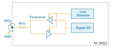
The NI 9402 has a maximum propagation delay of 55 ns and a typical propagation delay of 18 ns.
See Also
Update/transfer time, or Maximum update rate
Maximum signal switching frequency, or Maximum I/O switching frequency
Direction change time
Direction change time specifies the maximum time that it takes to change the line direction from input to output, or from output to input.
Example
The NI 9403 has a maximum direction change time of 18 µs. This means it can take up to 18 µs to change an input line to be an output line (or vice versa) and get valid data.
See Also
Input high current (IIH), or Input low current (IIL)
Ideally, the input impedance of a device is infinite and no current will be drawn, however this is not achievable in practice. When reading in a digital value at either 0 V or 5 V, a small amount of current will be drawn by the digital input circuitry of the NI module. The amount of current drawn while measuring a high voltage level is input high current, likewise the amount of current drawn while measuring a low voltage level is input low current. It is important to ensure that a digital signal being measured has the capability to tolerate the current values specified. This specification may also be listed under input and output voltage.
Example
The NI 9402 will either sink up to 100 µA when Vin = 0 V, or source up to 100 µA when Vin = 5.25 V. This applies to all digital lines.
Input high voltage (VIH), Input low voltage (VIL), or Input voltage
The recommended operating voltage ranges that an input signal should be to register a logic high or logic low.
Example
The NI 9401 specifies that the voltage input that will get recorded as a low signal ranges from 0 up to 0.8 V. For a high signal, this range is from 2 to 5.25 V. Below 0 V and above 5.25 V, the device is in the overvoltage protection state. An indeterminate range also exists where a change from low to high or high to low is not registered until they exceed the VIH or VIL.
See Also
I/O protection, or Overvoltage protection
Input high voltage (VIH), or Input low voltage (VIL), or Input voltage
Output high current (IOH), or Output low current (IOL)
When outputting a high or a low value, the nominal voltages for several NI modules are 0 V and 5 V. However, if a relatively low-impedance load is connected, a higher demand for current is present and this nominal voltage will rise from 0 V or fall from 5 V. This specification characterizes the relationship between the output current and the output voltage.
Example
The NI 9401 is capable of sourcing or sinking current depending on if a high value or a low value is written to the pin. The maximum value for sourcing and sinking current is either 2 mA or 100 µA per channel, depending on the output low and output high. When current is leaving the device (sourcing) the current is indicated as -2 mA. When current is entering the device (sinking) the current is indicated as +2 mA.
See Also
I/O protection, or Overvoltage protection
Individual digital lines have dedicated I/O protection against electrostatic discharge (ESD) and overvoltage conditions. For additional safety of the device, there is a second level of protection that is shared across all digital lines. Excess overvoltage on multiple lines at the same time stresses this shared protection circuit and may result in damage to the device. Continued use at this voltage level will degrade the life of the module.
Example
The NI 9401 has an overvoltage protection of ±30 V between the channel and COM pins on one channel at a time. This means that each line can individually handle up to ±30 V in overvoltage safely, but no more than one line at a time can exceed the nominal voltage input.
See Also
Input high voltage (VIH), or Input low voltage (VIL), or Input voltage
Short-circuit protection
The short-circuit protection defines at what condition the protection of the NI module will engage when in a short-circuit state. Each module specifies the response and the voltage or current threshold on a digital line that will engage the short circuit protection circuitry (this state is known as the short-circuit state).
Example
The NI 9476 specifies that the short-circuit protection will engage indefinitely when a channel is shorted to COM or to a voltage up to the value of the external power supply voltage. This means that if a digital line is accidentally shorted to COM, the channel will cycle off and on until the short circuit is removed or the current returns to an acceptably low level. Each channel of the NI 9476 has a status line that indicate in software whether the channel is in an overcurrent state.
Other Specifications
Calibration
Like all test and measurement equipment, it is important that routine calibration is performed to ensure that the module is operating within the specified accuracy settings. The module has some amount of self-heating, so it is important to allow the specified warm-up time prior to taking any measurements to ensure a stable temperature is reached. Once warmed up, it is recommended to perform a self-calibration, if supported. Refer to Calibration Services for more information about the calibration services that NI offers.
Example
The NI 9212 has a 15 minute warm-up time and a calibration interval of 1 year. After a year of use, NI recommends sending the module in for certified calibration.
See Also
What Are the Differences between Self-Calibration and External Calibration?
Environmental specifications
These specifications describe the conditions that the module is warranted to work in. Chassis, controllers, and backplanes are rated separately, so verify that all components of your system meet the specifications for your environment.
Example
The NI 9250 has an operating temperature range of -40 °C to 70 °C, and a maximum altitude of 5,000 m.
Environmental management
For more information about NI's commitment to design and manufacture products in an environmentally responsible manner, visit ni.com/environment.
Hazardous locations certifications
A hazardous location is an environment that contains potentially flammable or explosive material in the surrounding atmosphere. In North America, the class describes the nature of flammable material (e.g. gas, dust, etc.), the division describes what conditions the hazardous materials may exist under (normal or abnormal), and the group describes the specific type of material present (e.g. acetylene, hydrogen, etc.). Consult your module's user manual or getting started guide for cautions on operating in hazardous locations.
Example
The NI 9250 is certified for various locations, but specifically for UL Class I, Division 2, Group A as well as IECEx IIC. Both of these certifications are for locations where acetylene gas may be present.
See Also
MTBF
Mean time between failure (MTBF) is the average time between failure events for a repairable product. It is the mean number of life units during which all parts of the item perform within their specified limits, during a particular measurement interval under stated conditions. MTBF is a statistical estimate that is commonly used to calculate the probability of success (reliability) or the probability of failure for a product for a duration of operation in a defined environment.
See Also
What Is Reliability?
Where Can I Find the MTBF for My NI Device?
Physical characteristics
NI publishes dimensional drawings of most products that can be used to check clearance prior to purchasing a module or creating a model of the system being created. Physical characteristics also describe the wiring requirements for terminal connections.
See Also
Dimensional Drawings
Power requirements
It is important to know the power requirements of your system so that the correct amount of power can be sourced. The values indicated in this section are for typical use and do not show the maximum power that a module may draw if used outside of specifications. NI sells power supplies that meet the recommended specifications, but you may use a third party or custom power supply as needed. Make sure that your power supply is suited for your environment, especially in hazardous or rugged conditions. Some C Series modules have additional power requirements separate from the backplane.
Example
The NI 9250 consumes 0.96 W maximum from chassis when in active mode.
See Also
Powering Your CompactDAQ System
Safety, Electromagnetic Compatibility, CE Compliance
C series modules are tested and in compliance with various standards, which are listed in the three sections of our specifications manuals. For more information on any standard, visit ni.com/certifications.
Example
You can view the compliance specifications for the NI 9212 by using the certifications search: NI 9212 - Product Certification - NI
Safety voltages – Isolation
Isolation specifications apply to what the module can handle between earth ground and the pins. Connections to C series modules are rated for various categories of voltages. Measurement Category CAT O, previously known as Measurement Category CAT I, is for measurements of loads, devices, or circuits that are not directly connected to MAINs, and are isolated. Measurement Category CAT II is for measurements that could be connected to MAINs or are not isolated from MAINs. For C Series Modules, their safety voltage ratings are for the specific connection (e.g. RS-485 Serial Port, etc.), so modules with high voltage ratings can be used in any chassis.
Example
Safely connect up to 30 V (Measurement Category I) across channel-to-earth ground on the NI 9250.
See Also
Isolation and Safety Standards for Electronic Instruments
Safety voltages – Overvoltage
Overvoltage specifications apply to what the module can handle between pins. Connections to C Series modules are rated for various categories of voltages. Measurement Category CAT O, previously known as Measurement Category CAT I, is for measurements of loads, devices, or circuits that are not directly connected to MAINs, and are isolated. Measurement Category CAT II is for measurements that could be connected to MAINs or are not isolated from MAINs. For C Series Modules, their safety voltage ratings are for the specific connection (e.g. RS-485 Serial Port, etc.), so modules with high voltage ratings can be used in any chassis.
Example
Safely connect up to 30 V across AI+-to-AI- on the NI 9215 with BNC.
Shock and Vibration
C series modules are tested to specific industry standards to ensure that stated accuracy per the specifications and device integrity is maintained over the stated shock and vibe specifications. It is important not to exceed these specified values to ensure correct and accurate operation of the module. All C series modules, as well as cRIO and cDAQ chassis, are tested for the same shock and vibration standards. However, meeting these specifications may require certain mounting or connection procedures, which are explained in your chassis' user manual.
Example
In order to meet the shock and vibration specifications for the NI 9250, you must panel mount the system.
Thermal dissipation
This quantifies how much power is dissipated under worst-case conditions. This includes situations when the module input voltage exceeds recommended input voltage (overvoltage).
Example
The NI 9250 has a thermal dissipation at 70 °C of 1.30 W maximum when the module is in active mode. This means that when the module is ready to acquire data, is acquiring data, or is currently in a fault state the module will dissipate at most 1.30 W.
Warm-up time
Some ADCs are very sensitive to temperature changes. By allowing the module to reach a steady state temperature, this sensitivity can be reduced, and a more accurate reading can be measured.
Example
The NI 9212 has a 15 minute warm-up time. This means it is recommended to wait for 15 minutes after the module is powered to begin using the module to take measurements, to ensure optimal accuracy.