Image Data Interface Test Challenges for Modern Focal Plane Array Systems
Overview
Modern Focal Plane Array (FPA) Imaging Detectors are simultaneously high resolution, high sensitivity, and high speed. The high-resolution and high-speed requirements often lead to the need for high-speed serial data busses through an advanced Read-Out IC (ROIC). In this white paper, you will learn how NI technology removes the need for custom engineering by using COTS modular instruments that are customizable and robust for validation and manufacturing. The NI modern approach will reduce costly redesigns across programs and speed time to delivery.
Contents
- FPGA Evaluation Board Approach
- Modular, Standards-Based Approach
- Off-the-shelf Instrument Approach
- Accelerated Development at Reduced Costs
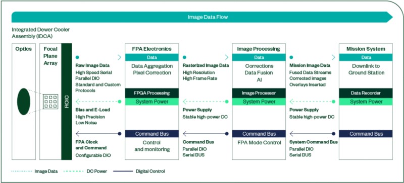
Figure 1: Common Imaging Detector System Architecture
Modern focal plane arrays (FPAs) often are customized to meet the unique requirements of a specific mission. However, most systems share a common overall system architecture, as shown in Figure 1. The FPA detector on the left is paired with advanced optics to capture incoming light from a specific wavelength range and convert that into pixels that are then converted into analog or digital data for further processing. Many times, the tightly integrated ROIC has three main interfaces for data, bias, and control. The data interface, shown above as the top path, can be a high-speed data bus (SerDes or LVDS) or an analog interface to offload image data. The FPA is powered and biased from a range of power supply lines represented by the center path on the diagram. These lines can have nonstandard voltage and loading requirements, depending on FPA device technology. Additionally, the FPA has a clocking and command interface, shown as the bottom path, to control the device during normal and testing operation. The data, bias, and control interfaces often cascade through other subsystems or circuit card assemblies. The FPA electronics, sometimes called the “close-in-electronics,” control the FPA, supply the bias, and consume raw frame data for correction and front-end processing. Teams often develop subsystems in parallel and those building the FPA device and FPA electronics must test interfaces before the other is ready, which challenges the FPA test engineer to emulate the digital interface functionality before it is ready.
The following sections present three approaches to test solution development and demonstrate the unique requirements of data interface testing while explaining an efficient solution based on NI modular FPGA-based high-speed instruments.
FPGA Evaluation Board Approach
Modern FPA testing requires moving large amounts of data through high-speed interfaces, often with some protocol customization to meet a specific mission requirement. Many FPA test initiatives leverage FPGA evaluation boards or custom interface boards to handle these high-speed interfaces. By using off-the-shelf FPGA evaluation boards, you can incorporate customized IP, which is often less expensive than acquiring FPGA silicon separately. However, evaluation boards often have short product lifecycles, making testers built on them a challenge to maintain long-term, adding to total test development and sustainment cost, especially if used in manufacturing test. Also, as devices age, software application updates may drop support for older devices, making obsolescence management a challenge. Additionally, in late stages of an FPA program or after placed in production, there is often significant risk of a tester failing and sustainment teams being unable to obtain replacement parts, forcing a late and costly tester update. Lastly, evaluation boards often require the skills of a specialized FPGA design engineer familiar with the low-level software implementation tools—a skill not often associated with test engineering experts.
Modular, Standards-Based Approach
An alternative to the custom approach with FPGA evaluation boards is the NI modular solution based on the PXI Express standard. The NI PXI Express instrument portfolio boasts several options to meet operational longevity requirements while retaining the ability to integrate custom digital IP. The NI solution for digital interface testing is based on FlexRIO technology. FlexRIO interface modules are commercial-off-the-shelf (COTS) instruments with a fully open FPGA as well as interfaces that meet the unique requirements of common FPA configurations. FlexRIO technology, when paired with LabVIEW FPGA development tools and built atop the Xilinx Vivado development platform, abstract some of the complexity of custom FPGA IP integration while maintaining a fully open user-programmable experience. FlexRIO devices often are paired with a high-capacity, high-speed storage RAID to record or play back data to the various subsystems.
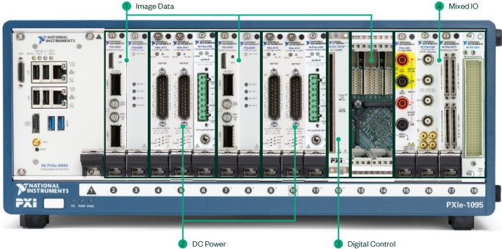
Figure 2: Common Imaging Detector Interfaces Mapped onto a PXI Express System
Figure 2 shows an example configuration using PXI Express modules that control interfaces common in FPA systems. Image data often connects to or from storage through a high-speed serial data interface module, using NI FlexRIO technology. Power and bias are controlled through various NI DC power supplies or a source-measure-units capable of providing power, measuring voltage/current, and adjusting load impedance. The system shown in Figure 2 is configured to support two parallel FPA digital and DC interfaces.
Off-the-shelf Instrument Approach
The design and manufacture of modern FPA subsystems share significant and increasing amounts of commonality between differing implementations. These similarities enable off-the-shelf solutions that can often accommodate 80% to 90% of typical test needs. NI Partner Viewpoint Systems has developed a 90% common solution called AEDIS. Based on NI FlexRIO and PXI products, AEDIS offers output (pitch) and/or input (catch) capabilities for handling high-speed digital imaging data streams, from configuring input data and clock channels, to signal conditioning, to ITA connectivity, all managed by software based on either a web UI or REST API for configuration and control. Business justification for an off-the-shelf instrument is typically based on risk reduction, schedule buyback (creating time savings), and cost abatement.
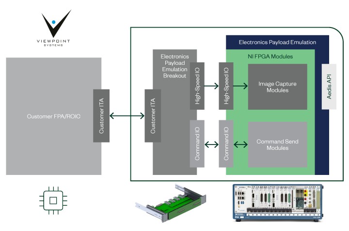
Figure 3: AEDIS Catch Instrument Block Diagram
Parallel Subsystem Test Development
The FPA subsystems in Figure 1 often are developed by different teams and—sometimes—different vendors. The team developing a specific FPA device may not be able to wait for the FPA electronics system to be available to test their new design. Similarly, engineers designing FPA electronics or mission software systems are required to test systems prior to the availability of the target FPA device. Parallel subsystem development is critical to efficient development but poses a challenge to test. A critical question is, how can you reduce the risk of failure at the integration stage before the rest of the system is ready?
Many engineers solve this challenge by using a customized digital interface solution to record, play back, or emulate data for the various FPA subsystems. Figure 4 illustrates how to interface NI hardware to test subsystems throughout the design cycle. Early-stage design may require full FPA system emulation to test mission software, whereas mid-design FPA sensor tests often are performed by recording data from an FPA device to characterize or calibrate image performance. A key benefit of the NI-based solution is that you can usually use the same hardware and software for all five scenarios represented in Figure 4— meaning that teams can standardize and share best practices and IP to accelerate development and test. As a concrete example, the AEDIS Pitch and Catch instruments use nearly the same hardware. In fact, both Pitch and Catch are often used together to speed parallel development by emulating both the FPA and the FPA electronics, permitting a jump on the design and development of I/O and interfacing components.
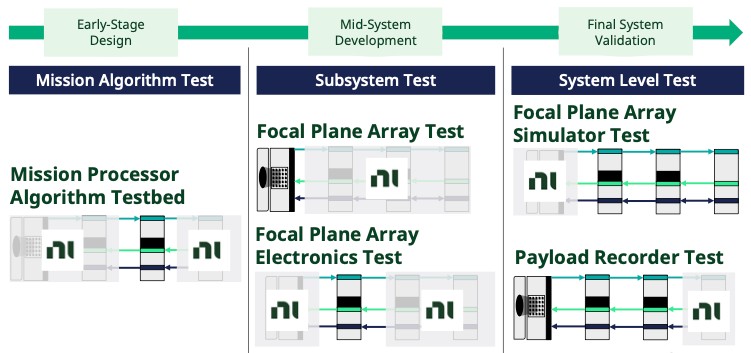
Figure 4: FPA Digital Interface Testing over the Development Cycle
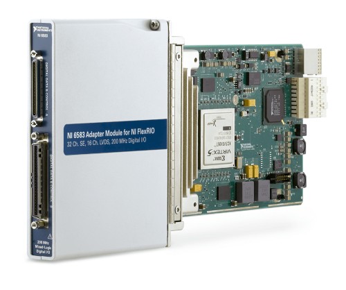
Figure 5: PXIe-7972 FlexRIO with NI-6583 Digital I/O Adapter Module
Parallel Data Interfaces
Many legacy FPAs use slow-speed, parallel digital input/output (DIO) interfaces, as the digitizer is integrated directly into the detector sensor or chip. These devices send digital data directly off the detector and commonly use standard logic levels such as transistor-transistor logic (TTL), low-voltage TTL, or low-voltage differential signaling (LVDS) for command and control. These devices tend to be slower speed and require parallel DIO test hardware for device capture and control. Figure 5 shows a common solution using an FPGA-enabled FlexRIO instrument, such as the PXIe-7972, with a digital adapter, such as the NI-6583.
SerDes-Coupled Interfaces
The most modern FPA detectors are designed with serial/deserializer (SerDes)-coupled interfaces integrated into the detector. These sensors can utilize standard physical layer protocols such as Serial RapidIO or Aurora, but may have some customized aspects, including data-framing changes. These changes can make interface testing a challenge. In addition, because of the high-speed nature of the interface, it is common to break the FPA into multiple segments requiring multiple high-speed serial interfaces. By separating an FPA into segments, interfaces can operate at lower rates, which may also ease performance requirements on cabling and connectors. However, test systems must account for the interface segmentation and protocol customizations. You can interface with these high-performance serial interfaces with the FlexRIO PXIe-6594 shown in Figure 6. The PXIe-6594 includes a fully open FPGA, like all FlexRIO-based modules, and includes two four-lane QSFP+ interfaces boasting speeds up to 28 Gb/s. Being a fully customizable FPGA-based instrument, it can support almost any serial interface protocol such as 1/10/100 Gigabit Ethernet, Aurora, Serial RapidIO, and more. The NI FlexRIO interface hardware can integrate your custom IP or third-party IP designed using LabVIEW FPGA, VHDL, or Verilog, or simply by importing an RTL block. Often signal interfaces to an FPA/ROIC interface have customized and specific electrical and mechanical requirements, so the Viewpoint AEDIS system is built to accommodate this requirement with an FPA interface module that is fully customizable for program specific requirements.
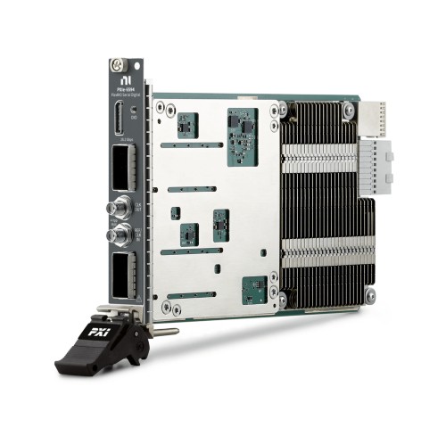
Figure 6: PXIe-6594 High-Speed Serial FlexRIO Module with Eight Lanes, up to 28 Gb/s
FPGA Software-Development Tools
If you’re designing with Xilinx-based devices, Vivado is a popular development platform that comes with a wide range of IP blocks that you can reuse. FPGA evaluation boards often come with a low-level board support package that requires digital design expertise to utilize. Frequently, engineers who are expert FPGA designers aren’t expert test-system designers. Therefore, maintaining custom FPGA IP for test can be a challenge from an operational staffing perspective.
The NI solution uses a graphical programing environment comprised of LabVIEW and the LabVIEW FPGA Module. LabVIEW FPGA is a development framework built atop Xilinx Vivado that provides an easier-to-use, high-level abstracted design flow while also retaining the ability to import custom FPGA IP. Figure 7 illustrates merging a custom HDL code into some LabVIEW FPGA code with a component-level IP (CLIP) integration node and targeting a high-performance FPGA-based PXI Express instrument. With the LabVIEW FPGA CLIP node, you can communicate over standard digital protocols while modifying digital interfaces, as with an FPGA evaluation board.
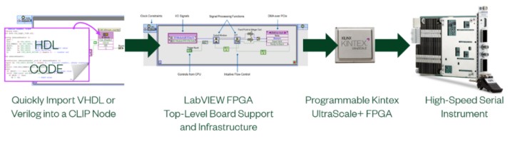
Figure 7: PXIe-7972 Module for FlexRIO with an NI-6583 Digital I/O Adapter Module
Think of LabVIEW FPGA as a higher-level, robust board support package that abstracts the most complex, expensive, and time-consuming aspects of FPGA design, such as incorporating PCI Express interfaces, direct memory access engines, peer-to-peer (P2P) FIFOs, and memory-mapped registers. The higher-level abstraction saves time so that you can focus on your IP and test challenges rather than board support infrastructure. A seemingly simple high-level block diagram can replace thousands of lines of VHDL code, vastly simplifying development and boosting productivity. For engineers who are more comfortable developing in traditional HDL languages, LabVIEW exports projects to Vivado so that you can develop with NI hardware while using the Xilinx tool chain.
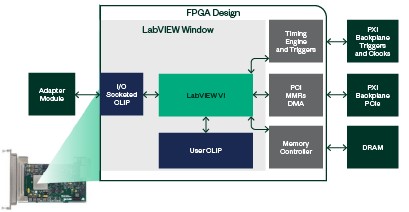
Figure 8: FlexRIO FPGA High-Level Block Diagram—A Robust Board-Support Package
Large Data File Transfer and Storage
As we discussed, digital FPA interface boards often are paired with a PXI system with copious RAM and/or a mass storage device such as an in-chassis or external RAID to store from or transmit data into one of the FPA subsystems. However, the large file sizes recorded or played back mean that standard computer system memory, or FPGA block RAM, may not be sufficient for some FPA test applications. Either way, you must have code in place on the host computer to manage moving data between the FPGA and a large data store. Having a system with data-movement capability in hardware is crucial to keep up with high sustained data rates to and from FPA devices under test.
Primary considerations for selecting a mass storage solution include data rate and capacity. Standard hard drives or solid-state drives typically can’t keep up with the data rates required for FPA test. To overcome this challenge, systems use high-performance streaming mass storage devices in a RAID 0 configuration. Two popular NI solutions are the NI PXIe-8267 Figures, there are other external alternatives in market as well. The PXIe-8267 conveniently is integrated into the PXI Express chassis; however, it is limited to 4 TB of storage, whereas the RMX-8268 is external, can be MXI-cabled, and can store up to 48 TB.
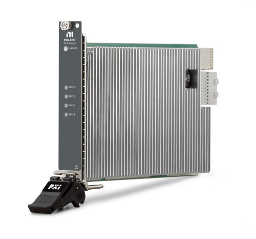
Figure 9: PXIe-8267 with 4 TB In-Chassis Mass Storage RAID
When reading and writing data to mass storage, it is best to minimize the number of times data is copied and moved within the system. The NI PXI Express system can bypass any extra copying by providing direct P2P data transfers between modules directly over the PXI Express backplane. Furthermore, Zero Copy methods move data directly between the FPGA and the RAID device. Learn more about implementing Zero Copy or P2P in your FPA test system.
Accelerated Development at Reduced Costs
Modern focal plane arrays operate with high resolution and can have high frame rates, requiring advanced high-speed data interfaces to move the copious amount of data. The NI solution for high-performance, serial interface test retains the openness and flexibility of using an FPGA evaluation board, but with more built-in functionality—crucial to modern FPA interface testing. The NI PXI Express-based solution uses FlexRIO modules covering a range of protocols and can stream P2P and Zero Copy for mass storage. With these advanced features and predeveloped instruments like AEDIS, engineers across the test engineering team can standardize and share best practices to accelerate program schedules and deliver capabilities on time—at a reduced cost and with improved readiness.
An NI Partner is a business entity independent from NI and has no agency or joint-venture relationship and does not form part of any business associations with NI.