Power Management IC Testing Using PXI Modular Instruments
Overview
Power management ICs (PMICs) are integrated circuits used to manage or convert power within systems such as a cell phones, tablets, or automotive ECUs. Low-power PMICs, such as those used in cell phones and other handheld devices where space is limited, mount directly to a PCB and are the crucial interface between the device’s power supply or battery and its complex electronics. A DC-DC power converter is one example of a commonly available PMIC used in a diverse range of applications where a power-converting circuit is used to upconvert or downconvert a source of direct current from one voltage level to another. Whether performing design validation prior to manufacturing or evaluating a DC-DC converter for possible use in a product, you need a repeatable and precise test sequence.
Standard DC-DC converter test sequences measure performance criteria such as voltage accuracy, efficiency, line/load regulation, and transient response. This paper examines how NI System SMUs have the power, precision, and speed to perform many of the tests that traditionally require a power supply, DMM, and oscilloscope.
Contents
- Example Component
- Current Consumption
- Application of Load
- DC Range and Accuracy Tests
- Transient and Noise
- Test System Expansion and Automation
- Recommended Hardware
- Next Steps
Example Component
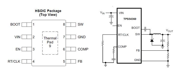
Figure 1: The Texas Instruments TPS54360 Step Down DC-DC Converter (Courtesy of TI.com)
For the purpose of discussing system setup and test procedures for a typical low-power DC-DC converter, consider the TPS54360 from Texas Instruments. The TPS54360, shown in Figure 1, is a step-down converter for automotive and communications systems. It can take an input voltage of 4.5 to 60 V and downconvert this to an adjustable 0.8 to 58.8 V output. Its maximum output current is 3.5 A.
By examining each of the TPS54360 DC-DC converter's specifications, you can determine which hardware you need to validate these values.
Current Consumption
When supplying a voltage that models the incoming battery feed voltage, many engineers are concerned about the current drawn by the DC-DC converter. Two specific currents of interest are the shutdown current and the quiescent current of a device.
Shutdown Current — To operate the MAX8640Y DC-DC converter, a voltage must be connected to the SHDN pin. Connecting SHDN to GND or logic low places the chip in shutdown mode. Manufacturers may be interested in the supply current that the converter draws from the source while in this state, referred to as shutdown current.
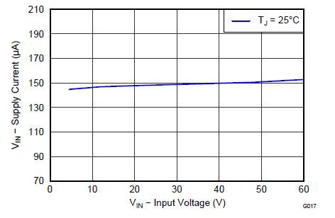
Quiescent Current — Quiescent current is the current drawn from the supply when no load is present on the other side of the DC-DC converter. To characterize this, a test engineer can monitor the power consumed on the input pin as a result of sweeping the supply voltage in 100 µV increments. The results of this might be similar to the graph seen in Figure 2.
Figure 2: Characterization of Quiescent Current for the TPS54360
| Parameter | Test Conditions | MIN | TYP | MAX | Unit |
|---|---|---|---|---|---|
| Supply Voltage (VIN Terminals) | |||||
| Shutdown supply current | EN = 0 V, 25 °C, 4.5 V ≤ VIN ≤ 60 V | 2.25 | 4.5 | µA | |
| Operating: nonswitching supply current | FB = 0.9 V, TA = 25 °C | 146 | 175 | ||
Table 1: Specification of Currents Drawn from the Supply as seen in the TPS54360 Data Sheet
As you can see in Table 1, the TPS54360 draws a typical shutdown current of 2.25 μA and a typical quiescent current of 146 µA.
Building Your Test System
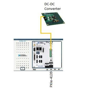
A good option for testing current consumption is the NI PXI-4139 precision source measurement unit (SMU), shown in Figure 3. This module is capable of both supplying the input voltage for the chip and measuring the current that the chip draws while connected. The PXI-4139 features a current measurement resolution of 100 fA in the 1 µA range, which is more than sufficient for characterizing quiescent and shutdown currents as well as leakage currents in the nanoAmp range. You can use this precision source in the DC-DC converter test system to perform programmatic sourcing and sweeping along with high-accuracy measurements.
Figure 3: An NI PXIe-4139 Added to Slot 1 of a Test System
In the next sections, learn how to build on this PXI system by adding one more PXIe-4139 and expanding the functionality. By the end of this paper, you should know how to create a complete PXI system with all the hardware necessary for testing DC-DC converters.
Application of Load
DC-DC converters were specifically designed to supply power to another device called the load. In DC-DC converter applications, load current is specified as the current that the circuitry downstream draws from the DC-DC converter at a specified power level. With the application of a load on the output side of the converter, you can now characterize a number of common industry specifications, including efficiency versus load curves, DC line regulation, DC load regulation, and current limit tests.
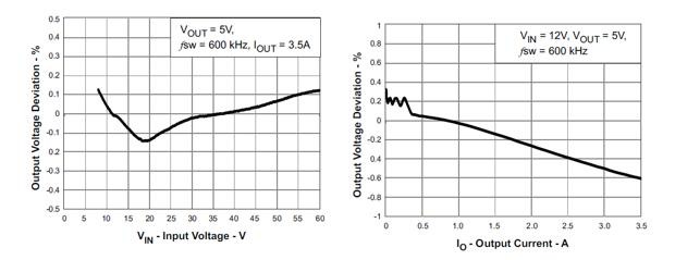
DC Line and DC Load Regulation — When the supply voltage seen by the DC-DC converter is swept from the rated maximum to the rated minimum while the chip’s outputs are held at the full current load, the output voltage changes. DC line regulation is the percent change in output voltage, expressed in mV/V or percentage. Similarly, DC load regulation is the change in output voltage, expressed in mV/A or percentage, as supply voltage is held steady and the output load is varied from a specified minimum rated current to the maximum rated current, or full load. Load regulation is typically measured when supply voltage is held at the nominal input voltage. Using an SMU to provide different loads, you can characterize this specification with a graph similar to that in Figure 4.
Figure 4: DC Line (left) and Load (right) Regulation as seen in the TPS54360 Data Sheet
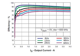
Efficiency versus Load Curves — Efficiency is the ratio of power consumed to power delivered, typically expressed as a percentage ([Vout * Iout]/[Vin * Iin] * 100). An efficiency versus load curve, therefore, illustrates how the efficiency of the DC-DC converter varies as the load increases. You may be interested in displaying a family of efficiency versus load curves, one for each minimum, nominal, and maximum input voltage. Figure 5 shows the efficiency versus load curve for various supply voltages of the TPS54360.
Figure 5: DC Load Regulations seen in the TPS54360 Data Sheet
Current Limit Tests — Peak output current limiting protects the DC-DC converter by ensuring the output current is limited to a predetermined maximum value under overload and/or short circuit conditions, both of which you can simulate during a test.
Building Your Test System
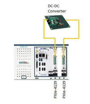
You should use an SMU during all of these tests so you can vary the current load being drawn from the DC-DC converter. The four-quadrant capability of the PXI-4139 means that you can use a second PXI-4139 SMU to provide the DC-DC converter with a load, as seen in Figure 6. The PXI-4139 can sink up to 12 W continuously while measuring the output voltage of the converter.
Figure 6: Adding the Second PXIe-4139 SMU to Your Test System in Slot 3
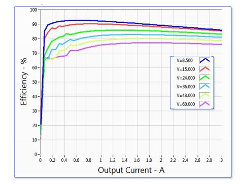
Using the hardware sequencing engine of the SMU and built-in triggering of the PXI chassis, you can synchronize the source and measure actions of both SMUs. This allows you to quickly test the DC converter at various input voltages and output currents as in the figure below, and execute large sequences with hardware-timed output.
Figure 7: Efficiency Plot of the TPS54360 with NI SMUs
DC Range and Accuracy Tests
The next performance criteria you need to consider when building a test system is the measurement of the DC-DC converter’s voltage accuracy. Due to the sensitive nature of the circuitry being powered by the converter’s output, you want to ensure that the voltages these downstream components see are as accurate as possible.
DC Range Tests — Output voltage range specifies the voltage range that the DC-DC converter can supply under full load conditions. As discussed previously, the output voltage varies because of changes in the supplied input power and the load. You can therefore characterize this range specification by measuring the converter’s output voltage as the load is held steady and the input is swept from the maximum to the minimum voltages it can support without damage. The TPS54360, as a step-down power converter, can receive a voltage range of 4.5 to 60 V and output a range of 0.8 to 58.8 V, as shown in Table 2.
DC Accuracy Tests — The output voltage accuracy specification of a DC-DC converter denotes the maximum variation of the output voltage when operating at user-specified conditions. The accuracy varies because of changes in temperature and the passage of time, and it is typically returned as a percentage of the expected or nominal value. For example, the TPS54360’s internal reference voltage accuracy is specified as ±1 percent over a temperature range of -40 to 150 degrees Celsius.
| MIN | MAX | Unit | |
|---|---|---|---|
| VIN Supply Input Voltage | 4.5 | 60 | V |
| VO Output Voltage | 0.8 | 58.8 | V |
| IO Output Current | 0 | 3.5 | A |
| TJ Junction Temperature | -40 | 150 | °C |
Table 2: Specification of Range as seen in the TPS54360 Data Sheet
Building Your Test System
In the PXI system, one PXI-4139 is supplying the input voltage and a second PXI-4139 is acting as a programmable load. Therefore, the only measurement you need to make for the characterization of the previously described DC accuracies is the measurement of the converter’s output voltage. The second SMU is already measuring this voltage to prevent damage to the hardware due to an overvoltage situation as it sinks the DC-DC converter’s current. You can simply read this value from the hardware.
When designing this test system, note that you should take a voltage measurement at the output of a DC-DC converter on leads that do not carry load current. If load current is flowing through the measurement leads, this can result in measurements off by many millivolts. Another point to keep in mind when measuring the accuracy of a device is that the test equipment should be at least 10 times more accurate than the device under test. If this is not the case, you may measure the inaccuracy of the test equipment itself and not the accuracy of the device under test.
You can address both of these concerns with PXI-4139 remote sense capabilities. Remote sensing is the ability to measure voltage directly at the UUT, thereby eliminating the measurement error introduced by voltage drops across lead resistances. Because the remote sense terminals of the SMU have high input impedance, a negligible amount of current flows through these leads, reducing the effect of lead resistance and accurately monitoring the load voltage.
The PXIe-4139 can measure voltage at high accuracy and high precision, and is able to perform measurements with a single SMU module that once required an additional DMM.
| Device | Resolution | Accuracy |
|---|---|---|
| PXI-4071 DMM | 1 µV (10 V Range) | 125 µV (0.0012%) |
| PXIe-4139 | 1 uV (6 V Range) | 1.5 mV (0.025% in 6 V Range) |
Table 3: Comparison of Resolution and Accuracy Specifications for the PXIe-4139 SMU and PXI-4071 DMM
Note: For more information on how to determine the resolution and accuracy of a given device and range, refer to the specifications pages of that device on ni.com.
Transient and Noise
Transient response is the response of a system to a change of equilibrium. Manufacturers can use these charts to illustrate the voltage and current responses of the DC-DC converter upon startup and how it responds to changes in line and load, highlighting the DC-DC converter’s overshoot/undershoot responses and settling time.
Line-Transient Response — Line-transient responses demonstrate how the voltage and current on the output pins of the DC-DC converter respond to changes in the input voltage. As you increment and then decrement the input voltage, you can monitor the voltage to acquire a graph such as the one in the top right of Figure 7.
Load-Transient Response — Conversely, load-transient responses, on the top left of Figure 7, illustrate the time it takes for the output voltage to settle to the specified accuracy after the output current load changes. You can test different amplitude steps for a complete understanding of the load-transient response, which is critical for testing mobile phones and digital consumer products.
Startup Waveforms — With the PXIe-4139’s maximum sample rate of 1.8 MS/s, you can measure the minimum ON time of the DC-DC converter. This is the settling time, or the time it takes for the output voltage to reach the specified accuracy when the output is at full load. For instance, the minimum ON time is determined when the input voltage is increased from zero to the nominal voltage and a measurement is made of the time it takes the output to settle. The minimum ON time of the TPS54360 can also measured by enabling the EN pin while Vin is present. This can be seen in the bottom graphs of Figure 7.
Noise and Ripple — Noise and ripple are AC measurements made at the output of a DC-DC converter in either millivolts RMS or millivolts peak-to-peak. The output ripple voltage is a series of small pulses with high frequency content and is therefore typically specified in mV peak-to-peak. The two major sources of ripple and noise as seen on the output of a DC-DC converter are the switching noise generated by the converter and the line ripple from the source. For the line ripple, a DC-DC converter source provides some level of ripple rejection; any remaining ripple the converter sees appears at the load. The most common method of filtering output ripple is to add inductance in series and capacitance in parallel at the output of the converter, commonly referred to as an “LC network.” Because of the high-frequency content of the noise and ripple, you should use a digitizer with a high bandwidth for the measurement so that all significant harmonics of the ripple spikes are included.
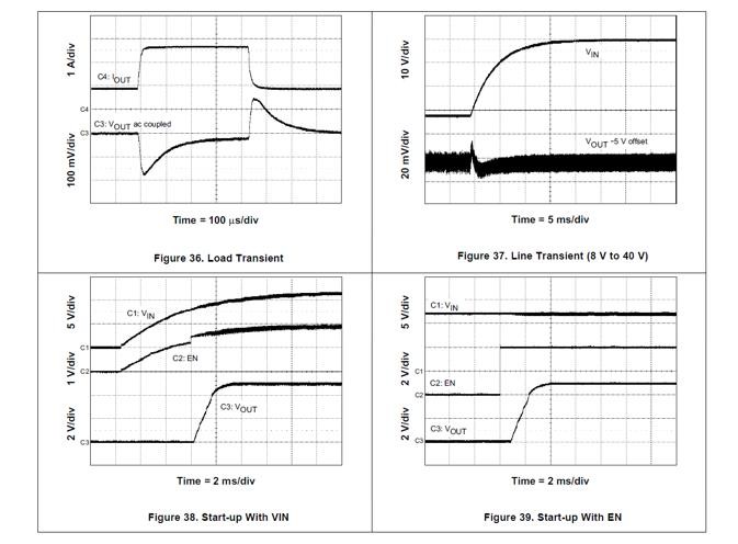
Figure 8: Load-Transient Response as seen in the TPS54360 Data Sheet (top left);
Line-Transient Response as seen in the TPS54360 Data Sheet (top right);
Start Up Waveforms as seen in the TPS54360 Data Sheet (bottom);
Building Your Test System
Traditional methods for performing transient and noise tests require probing the input and output lines of the DC-DC converter with an oscilloscope. However, the 1.8 MS/s sampling rate of the PXIe-4139 SMU is often fast to characterize line and load transients without the complication and cost of adding another instrument. Figure 8 shows the PXIe-4139 SMU measuring the load and line transient behavior of the TPS54360. In these tests, the SMU is acting as a precision DC power source, external load, and oscilloscope. The external load steps from 25% to 75% of its maximum current in a 500 µs pulse, and the SMU measures both the current draw and voltage output of the DC converter.
Note: Achieving a 500 µs pulse with a fast rise time and no overshoot or oscillation was made possible by using NI SourceAdapt technology, which is a digital control loop technology that allows you to control the transient behavior of the SMU.
Figure 9: Load and Line Transient Characteristics of the TPS54360 using NI SMUs
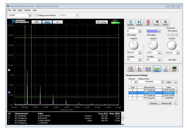
For higher speed acquisitions or spectral analysis, you can easily add a high-speed oscilloscope to your system in the peripheral slots of the PXI chassis. NI provides a wide range of PXI oscilloscopes, allowing you to optimize for high resolution or high speed measurements up to 24-bits of vertical resolution or up to 5 GS/s sampling in a single PXI slot. For example, by probing the input and output of the DC-DC Converter with the PXIe-5162 4-channel, 5 GS/s, 10-bit oscilloscope, you can examine frequency content of the noise using the Soft Front Panel. In this case, you can see several millivolts of switching noise around 600 kHz.
Figure 10: 2-Channel Frequency Plot using the PXIe-5162 Oscilloscope
Test System Expansion and Automation
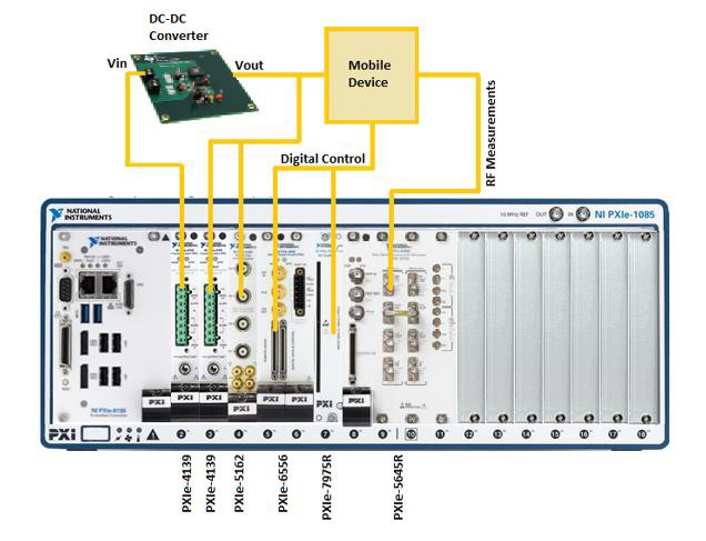
The PXI form factor offers you the ability to expand a test system. You can insert any number of additional PXI modules in the remaining slots of the PXI chassis. Some examples of hardware that test engineers often need when testing DC-DC converters include PXI modules capable of RF and mixed-signal functionality, high-speed digital I/O for timing analysis and interfacing, and FPGA-based I/O for closed-loop control and protocol-aware test.
With the strong integration of National Instruments hardware and software, you can implement PXI test system automation that achieves exact and repeatable timing for consistent data. You can easily write test sequences to step through the aforementioned specification tests using development environments such as NI LabVIEW software and then automate them with NI TestStand, a powerful ready-to-run test management environment.
Figure 11 shows an example of an expanded chassis.
Figure 11: Example of an Expanded Chassis
Recommended Hardware
A PXI system requires both a PXI chassis and integrated controller. For more information on PXI chassis and controllers, refer to What Is PXI?
The following hardware components were used in this system:
