Using the PXI-2593 50 Ohm RF Switch in a 75 Ohm Configuration
Overview
Contents
- Characteristic Impedance
- Example 1: Matched Source and Load
- Example 2: Matched Source, Switch, and Load
- Example 3: 50 Ohm Switch in 75 Ohm System
- Example 4: Video Signal Analysis without a Switch
- Example 5: Video Signal Analysis with a Switch
- Conclusion
- Additional Resources
Characteristic Impedance
The characteristic impedance of a switch describes the balance of distributed inductance and capacitance in a transmission line. It defines how a signal will propagate down the line. Maximum power is transferred when the output impedance of a source matches the input impedance of a load as shown in Figure 1. The R1 and R3 values are both 50 ohm.
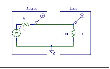
Figure 1. Ideal source-load system
Example 1: Matched Source and Load
In reality, the cable connecting the source and the load has a certain characteristic impedance. This impedance should match that of the source and the load as shown in Figure 2. In this case, both R1 and R3 are 75 ohm, and the impedance of the cable, Z0, is 75 ohm as well.
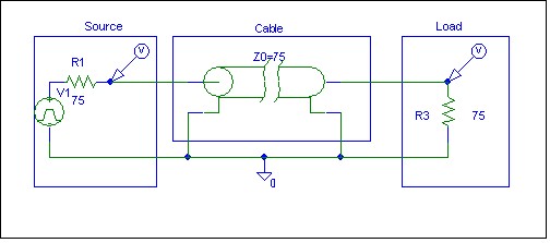
Figure 2. Source-Cable-Load with matched impedance
For simulation purposes, we can represent a high-frequency signal by a pulse with very short rise time (consequently have very high-frequency components). For this test setup, the cables connecting the source and load are RG-179 with solid Teflon dielectric. The propagation velocity though RG-179 is 69.4 % of the speed of light – therefore, the propagation delay though 1 m of RG-179 is:
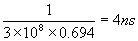
We will use 4 ns for the propagation delay though the cable. Voltages at the source and at the load for this impedance-matched system are represented in Figure 3. The horizontal distance between them is equivalent to the propagation delay.
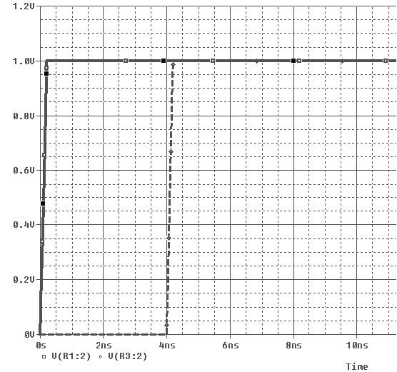
Figure 3. Voltage graph of system with matched impedance
Example 2: Matched Source, Switch, and Load
Many modern test systems involve a switching component that introduces another element in our ideally matched system. In this example, the switch has a characteristic impedance matching the other components (see Figure 4).
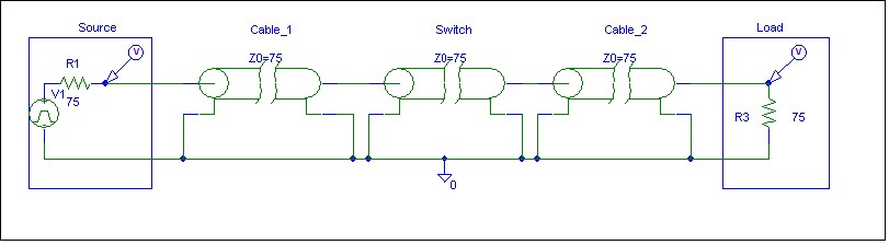
Figure 4. Switch with matching impedance is added to system
The propagation velocity though a switch can be calculated using the relative dielectric constant of the board dielectric (Er):

Let’s assume that the dielectric used in a PCB is glass-reinforced epoxy such as FR4 with a dielectric constant of 4. The propagation velocity is:
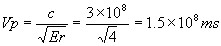
With traces of 15 cm, the propagation delay thought the switch is:
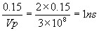
We will use 1 ns for the propagation delay through the switch. Voltages at the source and at the load for this impedance-matched system (with the switch) are shown in Figure 5. We can clearly see the additional horizontal delta added to our system from the propagation delay through the switch and the additional length of cable. Other than that, Figure 5 is identical to Figure 3.
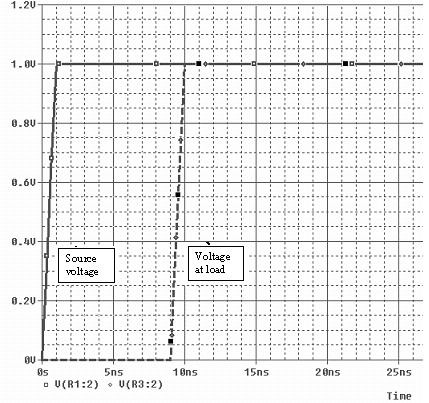
Figure 5. Voltage graph of system with matched impedance switch
Example 3: 50 Ohm Switch in 75 Ohm System
Now let’s analyze the effect of using a mismatched impedance component, like a 50 ohm switch, in the same system. The diagram of the new system is shown in Figure 6. All components are 75 ohm with the exception of the 50 ohm switch.
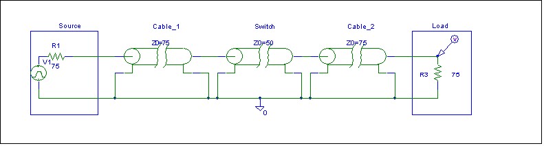
Figure 6. Switch with 50 ohm impedance added to the system
If we send the same signal we’ve seen in Figures 3 and 5 through this system, we will see the results as shown in Figure 7.
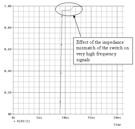
Figure 7. Voltage graph with unmatched switch impedance on a 500 MHz signal
The impedance mismatch of the switch created a step on the output voltage graph. The duration of the step is equal to twice the propagation delay of the switch. This is expected behavior – because of the impedance mismatch, a portion of the signal was reflected back to the source and is interfering destructively with the incident signal. This particular effect is often characterized by the term Voltage Standing Wave Ratio (VSWR) and is frequently specified on switch modules by themselves. In this case, it’s not the VSWR of the switch that is reflecting the signal back, but rather the impedance mismatch that’s creating the reflected wave. If the distortion caused by this effect is beyond the requirements of the application, it can be eliminated by matching the impedance of the system to the switch. The source must still have a characteristic impedance of 75 ohm, but every component including the load should now have a 50 ohm characteristic impedance (shown in Figure 8). This will minimize the distortion due to the impedance mismatch of the switch but will also result in a lower overall voltage measured at the load (due to the 75-50 ohm attenuation).
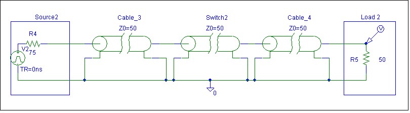
Figure 8. System with 75 ohm source, 50 ohm switch, 50 ohm cable and 50 ohm load
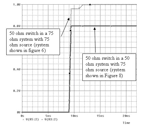
Figure 9. Voltage graph showing the difference between matched and unmatched impedances separate from the 75 ohm source at 500 MHz
Note that the distortion effect in the voltage graph appears only for signals with very high bandwidth. For instance, the dotted line in Figure 9 represents a signal with 500 MHz bandwidth. (On a signal with 30 MHz bandwidth, the dip only appears at 99.8% of the total voltage.) The same 500 MHz signal shows no visible dip when the other components of the system are matched at 50 ohms to meet the switch – only the reduction in total signal level. Because the reduction in total signal level can be calibrated out, the 50 ohm switch with 50 ohm cables and load can be an acceptable solution for testing high-frequency 75 ohm source outputs. Now, let’s look at a case that relates directly to video switching. The common NTSC format for video operates at around 6 MHz. Using this in the simulation from Figure 6, the rise time of the source is increased to 166ns.
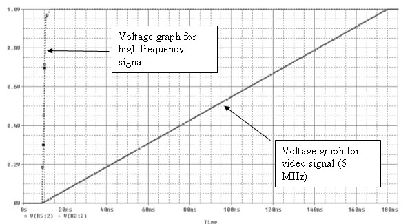
Figure 10. Voltage graph with mismatched switch impedance for high frequency signal and 6 MHz signal
In Figure 10, you can still see the previous high-frequency signal with the dip. The second plot, however, shows no effect on the voltage measured at the load of a 6 MHz signal. At lower frequencies, the destructive reflection interference described earlier is not present. (VSWR increases with frequency.)
Example 4: Video Signal Analysis without a Switch
To take this example further, an actual video signal has been analyzed. In this case, we generated an M-NTSC video signal from a color bar bitmap image (shown below) using the NI PXI-5431 video generator with the Composite Video Generator Software.

Figure 11. Color bar bitmap image used to generate M-NTSC video signal
To analyze the video signal we used the NI PXI-5122 100 MS/s, 14-bit digitizer with the Analog Video Analyzer software from microLEX System A/S; VideoMASTER. The NI PXI-5122 was connected to the NI PXI-5431 using 50 ohm cable with a 75 ohm feed-through terminator.
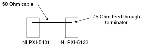
Figure 12. Source and digitizer connection
Color bar measurement performed by the VideoMASTER Analog Video Analyzer yields luminance and chrominance amplitude as well as chrominance phase. The measurements were saved into a file and shown below.
VideoMASTER Video Measurement Results File
*******************************************************
COLOUR BARS 7/21/2004, 4:36 PM
NTSC Composite Test Pattern = Colour Bars
White Bar Rise Time N/A
White Peak-to-Peak 998.3 mV
Luminance Amplitude:
White 713.6 mV
Yellow 637.6 mV
Cyan 515.2 mV
Green 440.4 mV
Magenta 324.8 mV
Red 250.2 mV
Blue 129.2 mV
Black 0.0 mV
Chrominance Amplitude:
Yellow 603.8 mV
Cyan 851.1 mV
Green 814.2 mV
Magenta 800.4 mV
Red 851.9 mV
Blue 607.6 mV
Chrominance Phase (+V):
Yellow 167.2 Deg
Cyan 283.6 Deg
Green 240.6 Deg
Magenta 60.6 Deg
Red 103.4 Deg
Blue 347.0 Deg
Yellow Bar Start 16.50 us
Blue Bar End 55.50 us
Example 5: Video Signal Analysis with a Switch
We placed an NI PXI-2593 between the NI PXI-5431 and the NI PXI-5122 and conducted the same color bar tests with the VideoMASTER analog Signal Analyzer as in example 4. Channel 0 was connected to Com 0 on the PXI-2593.
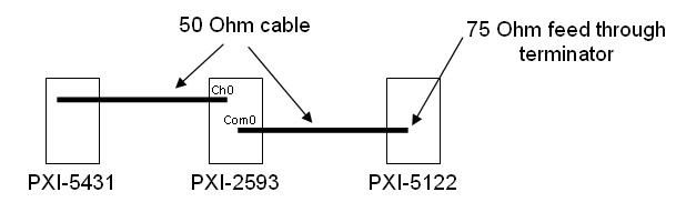
Figure 13. Source, switch, and digitizer connection
VideoMASTER Video Measurement Results File
*******************************************************
COLOUR BARS 7/21/2004, 4:47 PM
NTSC Composite Test Pattern = Colour Bars
White Bar Rise Time N/A
White Peak-to-Peak 992.9 mV
Luminance Amplitude:
White 709.9 mV
Yellow 634.8 mV
Cyan 512.3 mV
Green 437.4 mV
Magenta 323.1 mV
Red 249.2 mV
Blue 128.5 mV
Black 0.0 mV
Chrominance Amplitude:
Yellow 596.5 mV
Cyan 840.7 mV
Green 805.9 mV
Magenta 790.0 mV
Red 841.7 mV
Blue 599.4 mV
Chrominance Phase (+V):
Yellow 167.2 Deg
Cyan 283.5 Deg
Green 240.7 Deg
Magenta 60.6 Deg
Red 103.4 Deg
Blue 347.2 Deg
Yellow Bar Start 16.50 us
Blue Bar End 55.50 us
For easy comparison, we have listed all the measurements in Table 1.
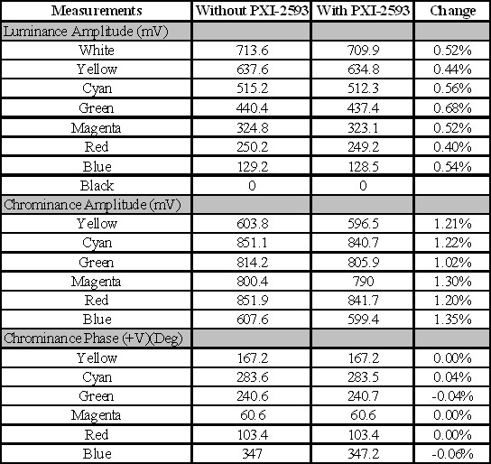
Table 1. Video signal measurements comparison
As this data demonstrates, the effect of the NI PXI-2593 in the system is minimal, accounting for what is often less than 1% change from the direct source-digitizer configuration. These results are similar to the impact expected from the introduction of any switch into a system as no switch represents a completely invisible introduction into the system.
Conclusion
For many of the most common applications (including NTSC video signals around 6 MHz), a switch with 50 ohm characteristic impedance can be used to switch video signals in a 75 ohm system. The effect of the impedance mismatch is very limited and will not introduce significant distortion at video signal frequency. However, as the data in this document has shown, the amount of distortion increases with frequency. Matching the “mismatched” impedance (in this case, 50 ohm) throughout the rest of the signal path, though, will leave you with a signal purely attenuated by a factor consistent with a 75-50 ohm attenuation. This resulting attenuation can be calibrated against, though, still providing a reasonable solution for 50 ohm switching in a 75 ohm system.
All switches will have some impedance mismatches internally, especially if they have “stubby” topologies such as in a matrix. These additional capacitive loads can result in distortions even if the specifications indicate the signal chain is perfectly matched.
Note: The NI 5431 Video Generator was declared end-of-life (EOL) in November 2007. It was later replaced with the NI Analog Video Generator solution. The VideoMASTER solution developed by microLEX was acquired by National Instruments, and is now packaged as NI Video Measurement Suite with the NI Analog Video Analyzer.