Interfacing NI PXI-655x Digital Waveform Generator/Analyzers to ECL Logic Families
Overview
- Single-ended ECL
- Differential ECL
- Using an off-board TTL-ECL translator
Interfacing to PECL (positive emitter-coupled logic) can be done using these same methods; however, you must change the acquisition and generation voltage levels of the PXI-655x. In fact, some ECL buffer chips can change between the two logic families by simply changing the polarity of their power supply.
Note: The ON Semiconductor MC100E116 was used in the examples in this document. NI recommends you use this or an electrically similar device when creating your application.
The following table summarizes the differences between the methods.
Connectivity | Noise immunity | Channels per PXI-655x | Additonal IC | |
| Single-Ended ECL | Easiest | Low | 20 | - |
| Differential ECL | Medium | Medium | 10 | - |
| Off-Board TTL-ECL Translator | Challenging | Excellent | 20 | √ |
Contents
- Method 1. Single-Ended ECL
- Method 2. Differential ECL (Generation Only)
- Method 3. Using an Off-Board TTL-ECL Translator
Method 1. Single-Ended ECL
Generation
From a connection standpoint, the simplest way to perform a pattern generation to communicate with an ECL receiver is with a single-ended interconnection. Though ECL is traditionally a differential standard, the single-ended configuration is well understood and commonly implemented. In this configuration, the single-ended signal is usually connected to the positive input of the differential ECL receiver, and the negative input is connected to a DC level at the midpoint of the single-ended signal swing as shown in Figure 1. Many ECL receivers offer a voltage reference pin (often called VBB or VTT) specifically for this purpose. The ON Semiconductor MC100E116 provides a VBB voltage of about –1.3 V. NI recommends single-ended ECL for interfacing to ECL receivers under all but the harshest environments.

Figure 1. Voltage Swing of Single-Ended Connection
The single-ended configuration is simple to implement. As you can see in Figure 2, it requires only a single connection to the ECL receiver and no additional termination is required. NI recommends using an SHC68-C68-D2 cable and a CB-2162 connection block to make this connection.
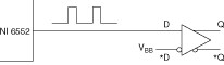
Figure 2. Standard Single-Ended Receivers with VBB
While this single-ended configuration produces reliable results in most environments, you do not get many of the advantages of differential data transmission. There is no common-mode rejection in the circuit to account for noise pick-up or system crosstalk. You also must ensure that the bias voltage on the negative input pin of the ECL receiver is stable. Even small fluctuations and ripple on this voltage can cause jitter in the ECL receiver. In addition, the signal interface window is essentially half of what it would be in a differential configuration, since the voltage difference at the receiver is between the mid (bias) point and the single-ended line.
Once your system is connected as shown in Figure 2, you must configure the generation voltage levels of your NI device. Consult the data sheet for your ECL receiver to determine how to set these voltage levels. Set the NI device generation voltage high to the typical VIH parameter on the receiver datasheet. Then, set the NI device generation voltage low to the typical VIL parameter on the receiver datasheet. For the MC100E116, VIH is -0.88 V and VIL is -1.475 V. Figure 3 shows LabVIEW code using NI-HSDIO, the driver software for the PXI-655x modules, to provide an example of how to program your generation voltage.
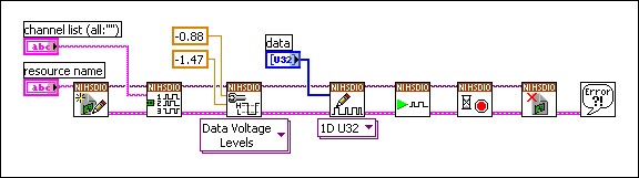
Figure 3. Example Code for Single-Ended ECL Generation
Acquisition
For acquisition, connect the positive output terminal of the ECL driver to a PXI-655x DIO channel. This connection should be terminated at the ECL driver before the signal enters the cable. With this termination scheme, you can set the input impedance of the PXI-655x to 10 kΩ, avoiding the voltage-divider effect that occurs with the lower 50 Ω setting. Refer to Figure 4 below for an illustration of how to make this connection. Resistors are added in front of the transmission line to bring the source impedance up to 50 Ω to match the cable. The 220 Ω resistor is required to provide a path for current to flow out of the emitter of the output stage. The value of the resistor can vary depending on the power constraints of the ECL driver.
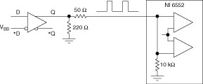
Figure 4. Single-Ended Acquisition Connection
Once your system is connected as shown in Figure 4, you must configure the acquisition voltage levels of your NI device in your application. For this application, both the acquisition voltage level high and low are set to the same value at the midpoint of ECL signal swing. To determine how to set these voltage levels, you should consult the data sheet for your ECL driver. Set the NI device acquisition voltage high and voltage low to the midpoint between the VOH and VOL parameters on the ECL driver datasheet. For the MC100E116, these voltages are -0.95 and -1.745 V, respectively. For these values, the acquisition threshold for the NI device would need to be ((-0.95) + (-1.745))/2 = -1.3475 V. Because the voltage resolution of the PXI-6552 is 10 mV, rounding this number to -1.35 V is acceptable. Be aware that if you are terminating with 50 Ω, you will likely need to adjust this voltage due to the voltage-divider effect that is described in more detail in the NI Digital Waveform Generator/Analyzer Help. Terminating with this low resistance can also cause your ECL device to operate beyond its specified power limits. Figure 5 shows example LabVIEW code that can program the PXI-655x for this voltage level.
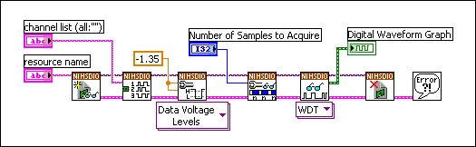
Figure 5. Example Code for Single-Ended ECL Acquisition
Summary
Advantages
-
You can use the full channel count of your PXI-655x module
-
Reduced power when compared to Differential ECL
-
Easier connection to the circuit
Disadvantages
-
Higher noise sensitivity
-
Poor receiver sensitivity
-
Higher jitter, phase error, and duty-cycle distortion
-
Reduced signal interface windows – difference is midpoint to level instead of level to level
Method 2. Differential ECL (Generation Only)
The second method for interfacing to an ECL device simulates a differential signal by using two channels of the PXI-655x. When generating patterns using this method, the PXI-655x always generates on two channels for every bit of information, and the two channels are always the inverse of each another. Figure 6 shows this connection, where Q and Q* represent two separate channels of the PXI-655x. Now the ECL receiver can compare between the full voltage swing instead of half the swing like in the single-ended ECL configuration. Programming for the differential ECL configuration is the same as for single-ended, but you must write inverse values to one channel in each of the pairs of channels that represent one single transmission line.
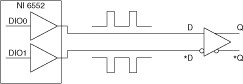
Figure 6. Standard Differential ECL Connections
Because the PXI-655x can only acquire single-ended signals, you do not gain any benefit from acquiring data with two channels. Connect your device as discussed in the Acquisition section for single-ended ECL.
Summary
Advantages
-
High common-mode noise rejection
-
Better receiver sensitivity
-
Less jitter, phase error, and duty-cycle distortion
-
Wider signal interface windows
Disadvantages
-
Only 10 lines per PXI-655x
-
Higher power when compared to Single-Ended ECL
-
More difficult connection
Method 3. Using an Off-Board TTL-ECL Translator
One way to generate ECL signals with the PXI-655x is using an external IC, such as the ON Semiconductor MC100H602 or an electrically similar device, designed to convert single-ended, TTL-level signals to ECL signals. Instead of individually choosing the high and low voltage levels for generation and acquisition, you can choose one of the defined logic families from NI-HSDIO (see Figure 7).
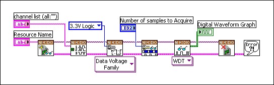
Figure 7. Example Code for Using an Off-Board TTL-ECL Translator
Summary
Advantages
- Gives the best possible ECL signal quality in terms of
- - Common-mode rejection
- Pulse-width distortion - Custom interconnections from the ECL Translator to the ECL device.
- Wide range of translator chips from a number of manufacturers so you can choose the price/performance you need for your ECL interface.
Disadvantages
- You must design and build a special interface circuit.
- You may need an additional power supply (or supplies) to power the interface circuit.
- Interface circuit increases the cost of the system
Related Links:
NI Digital Waveform Generator/Analyzer Help