Advanced Data Acquisition Techniques with Multifunction Reconfigurable I/O Hardware
Overview
Multifunction reconfigurable I/O (RIO) devices, previously called R Series devices, feature user-defined, onboard processing for complete flexibility of system timing and triggering. Instead of a fixed ASIC for controlling device functionality, multifunction reconfigurable I/O devices use an FPGA-based system timing controller to make all analog and digital I/O configurable for application-specific operation. You can implement completely flexible and customized data acquisition (DAQ) tasks using multifunction reconfigurable I/O hardware and the NI LabVIEW FPGA Module.
Contents
- Introduction
- Timing and Triggering
- Synchronization
- Analog Waveform Generation
- Counter/Timer Operations
- Data Transfer Methods
- Conclusion
- Next Steps
Introduction
Using LabVIEW FPGA, DAQ system developers have complete flexibility when programming an application for any type of input/output operation. Without having any prior knowledge of hardware design tools such as VHDL, you can embed LabVIEW code onto an FPGA chip and achieve true hardware-timed speed and reliability.
Let’s begin by addressing the common components of DAQ hardware. Assuming you’ve got analog-to-digital converters (ADCs), digital-to-analog converters (DACs), and digital input/output lines, all the I/O needs to be timed and controlled somehow for actual operation. Typical multifunction DAQ devices use a feature-rich ASIC that incorporates the majority of needs in functionality. Reconfigurable devices are differentiated from all other DAQ devices on the market because instead of a fixed ASIC for controlling device functionality, they use an FPGA-based system timing controller to make all analog and digital I/O configurable for application-specific operation. The reconfigurable FPGA chip is programmed with the LabVIEW FPGA Module, where the LabVIEW dataflow paradigm still applies, but with a new set of functions that control device I/O at the lowest level. Instead of abstracting out common tasks and functions with the NI-DAQmx functions, LabVIEW FPGA I/O nodes work at the most fundamental level with complete flexibility on all channels. In the following sections, examine specific NI-DAQmx examples and explore how to customize various data acquisition tasks using reconfigurable hardware.
Timing and Triggering
The most common use of reconfigurable I/O for advanced data acquisition is custom timing and triggering. Below is an example block diagram of a triggered analog input task using NI-DAQmx.
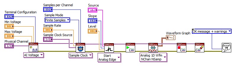
Figure 1. Triggered Analog Input With NI-DAQmx
Instead of using different functions for channel configuration, as shown in Figure 1, this hardware uses functions called FPGA I/O nodes for the reading and writing of all analog and digital channels. Let’s look at the exact same functionality using I/O nodes in LabVIEW FPGA.
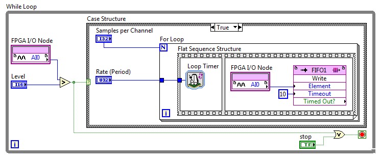
Figure 2. Triggered Analog Input With R Series and LabVIEW FPGA
You can see that there are no configuration functions for global channels; sample clocks; triggers; or starting, stopping, and clearing tasks. It’s all been replaced by a simple analog I/O read, and all timing is controlled by native LabVIEW structures such as While Loops and Case structures. Because the entire block diagram executes in FPGA hardware, the LabVIEW code executes with hardware-timed speed and reliability. Let’s look a little deeper into how this block diagram works. Instead of specifying a particular sampling rate, the analog I/O node uses the For Loop to acquire each sample. The corresponding ADC actually digitizes the input signal when the FPGA I/O node is called, and is therefore clocked by the For Loop. If you wanted to sample a signal at 100 kHz, the delay specified for that loop should be set to 10 µs. The loop timer function ensures a specific delay in time, beginning with the second loop iteration, so we’ve used a sequence structure to ensure the specified time period between samples. The Case structure in LabVIEW FPGA is powerful, because it essentially represents a hardware trigger for all the code it encapsulates. With all functions and structures executing in hardware with gates of logic, the Case structure ensures that the sampling begins at the correct moment in time, within 10 µs of accuracy. Lastly, there is no need to clear the task ID or release memory, because we are now working at the hardware level with few layers of abstraction.
The true benefits to using FPGA-based hardware is the ability to customize all timing and triggering, as well as implement signal processing and decision making in hardware. Let’s now see what it takes to modify our analog input trigger for some custom application. What if we wanted to trigger the acquisition if either of two analog input channels exceeded a certain threshold? This is fairly simple to implement in LabVIEW FPGA.
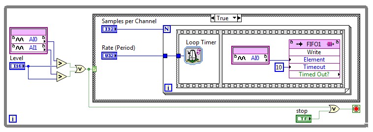
Figure 3. Custom Triggered Analog Input With R Series and LabVIEW FPGA
You can see that we added a second FPGA I/O node and a second compare function, as well as a Boolean OR function to the block diagram. R Series boards have dedicated ADCs on every analog input channel, so both channels are sampled simultaneously, and if either of those exceeds the specified limit the Case structure executes the true case and begins the acquisition within the same 10 µs of accuracy. Keep in mind that it’s not possible to generate a trigger like this on hardware enabled by NI-DAQmx. You could implement this type of trigger in software, but this would require software-timed decision making with much higher latency. If we wanted to then expand this from monitoring two channels to all eight channels, or even add digital triggers, the customized code wouldn’t be any more complicated. Adding pretrigger scans would involve constantly sampling the input channel and passing data into a first-in-first-out (FIFO) buffer. Once the trigger was read, the FIFO buffer and subsequent samples would then be passed to the host through a DMA channel.
If we wanted to sample a second analog input channel using the NI-DAQmx driver, the block diagram wouldn’t be much different than what is shown in Figure 1. There would still be limitations, however, because both channels would be forced to reference the same trigger and sample at the same clock rate. Let’s look at the different options for sampling multiple channels using reconfigurable I/O and LabVIEW FPGA.
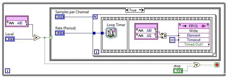
Figure 4. Triggered Simultaneous Analog Input With R Series
Figure 4 (above) shows us how to simultaneously sample from two different analog input channels, based on an analog trigger from analog input channel 0 (AIO). Since all multifunction reconfigurable I/O devices have independent ADCs, two channels within an I/O node are sampled at the exact same instant. Typical multifunction DAQ devices multiplex all channels through a single ADC, and therefore all channels must share the same Sample Clock and trigger lines. Figure 5 (below) shows that multifunction reconfigurable I/O devices can actually sample different analog input channels at independent rates. By placing the analog input I/O nodes within independent loops, each channel can sample at completely different rates, and then stream data independently through two DMA channels.
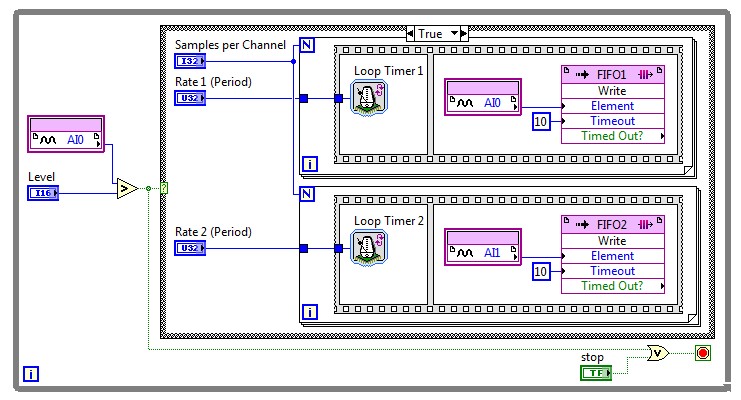
Figure 5. Triggered Multirate Analog Input With Multifunction Reconfigurable I/O Hardware
Lastly, if we wanted both channels to have independent sampling rates, as well as independent Start Triggers, we could place each I/O node in parallel loop structures as shown in Figure 6. This takes full advantage of FPGA parallelism, where each task uses its own dedicated resources and executes completely independent of any other acquisition task.
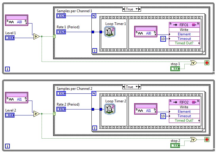
Figure 6. Independently Triggered, Multirate Analog Input With Multifunction Reconfigurable I/O Hardware
Synchronization
There are many synchronization options built into the NI-DAQmx driver for correlating inputs and outputs in time. Below is the block diagram of an analog input channel and analog output channel synchronized with a digital start trigger, done by specifying a digital trigger for the analog input and using the analog input start trigger signal to trigger the analog output generation.
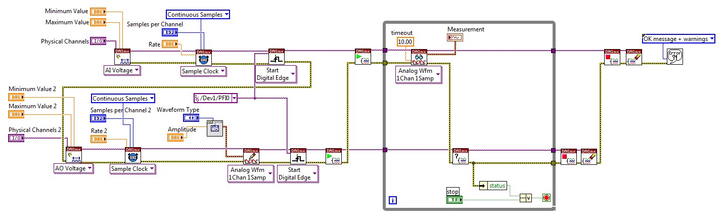
Figure 7. Synchronized Analog Input and Output With NI-DAQmx
To implement the same synchronization scheme with multifunction reconfigurable I/O hardware is fairly simple without the need for task IDs and onboard signal routing. Here’s how this would look on the LabVIEW FPGA block diagram.
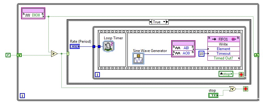
Figure 8. Synchronized Analog Input and Output With R Series
Once again we’re using the Case structure to implement a hardware trigger on the FPGA chip, and a rising edge on digital channel 0 initiates code in the true case. The analog input and output nodes are called simultaneously within the sequence structure with almost no jitter, and if we wanted them to have independent rates, we could easily place the analog I/O nodes in their own separate While Loops. It’s also important to note that the sine generator function shown in this block diagram is an express VI with which you can interactively configure the sine values in a look-up table.
The block diagram shown in Figure 8 has the same functionality as the NI-DAQmx VI in Figure 7, but if we wanted to customize this task, only a reconfigurable I/O device would provide the flexibility to do so. If we needed to add a Pause Trigger, for example, it could be easily accomplished by adding a Case structure within the inner While Loop and using another digital I/O node to select a true or false case. The power to program hardware provides endless possibilities for I/O timing and synchronization.
Another example of multifunction synchronization is generating finite pulses with the onboard counters and using the counter output as the analog input sample clock. This process is the common approach to implementing a retriggerable finite sample acquisition. Below is the required NI-DAQmx code for such an acquisition.
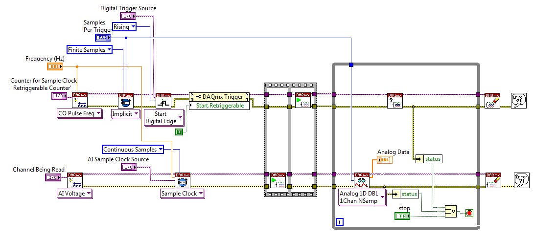
Figure 9. Retriggerable Finite Analog Input With NI-DAQmx
Now let’s compare this to a LabVIEW FPGA block diagram with the same functionality.
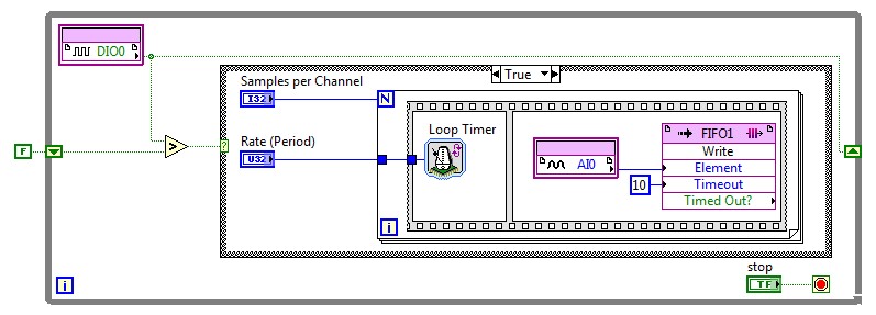
Figure 10. Retriggerable Finite Analog Input With R Series and LabVIEW FPGA
It’s obvious in Figure 10 that there are far less driver configuration steps due to the fact that the LabVIEW code executes in hardware. With a simple digital input line and For Loop structure, we’ve created hardware-retriggerable finite acquisition. The previous block diagram in Figure 9 uses two onboard counters to create the retriggerable finite pulse train, and typical multifunction DAQ devices have only four counters to work with. Multifunction reconfigurable I/O devices, however, can configure any digital line to be a counter using LabVIEW FPGA. We’ll cover more on counter/timer implementations in a later section.
We could take the hardware-timed flexibility of reconfigurable I/O devices one step further with a frequency-triggered acquisition. While this isn’t possible with a typical multifunction DAQ device, the high-speed onboard decision making can be used to calculate the frequency of an input signal and then select the desired code within a Case structure. For multiple device synchronization, multifunction reconfigurable I/O devices can also use the RTSI bus for PCI/PCI Express boards or the PXI trigger bus for PXI modules. These external timing and synchronization lines can also be accessed through FPGA I/O nodes on the block diagram.
Analog Waveform Generation
Many multifunction DAQ devices have analog output channels that implement a FIFO buffer for continuous analog waveform generation. The waveform being generated can use the FIFO as a circular buffer, and continuously regenerate a series of analog values without any further updates from the host. This relies less on the availability of the communications bus because data isn’t constantly being streamed to the device. If the waveform needs to be modified, however, the output task must be restarted in order to write new data to the FIFO. The other option is to continuously stream data to the hardware FIFO, which can lead to latencies in your output task. Multifunction reconfigurable I/O devices give you the ability to store the waveform outputs in hardware, and even use hardware triggering to change waveforms, thereby creating an arbitrary waveform generator.
Below is an example of a function generator that uses digital input lines to trigger changes in the output waveform. Based on the combination of digital I/O lines 0 and 1, we get four different states, or cases for analog output.
Figure 11a. Function Generator With R Series Case 0—Zero Output
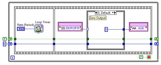
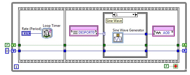
Figure 11b. Function Generator With R Series Case 1—Sine Wave
If both lines are low, Case 0 is executed and as shown in Figure 11a, the output is a constant value of 0 V. If DIO line 0 is high and DIO line 1 is low, Case 1 executes and generates a sine wave on analog output 0. This sine generation case (Figure 11b) uses the sine generator Express VI with which you can interactively configure a sine waveform with the required integer values in LabVIEW FPGA.
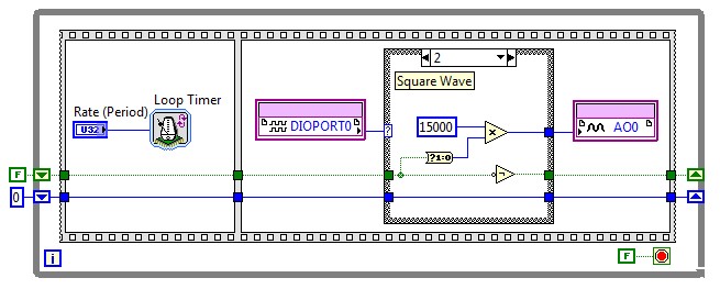
Figure 11c. Function Generator With R Series Case 2—Square Wave
Case 2 (Figure 11c) simply toggles a Boolean value on every iteration of the While Loop. If the value is low, integer 15000 is written to the analog output 0, which corresponds to value 15000 in the output register of a 16-bit DAC. A signed 16-bit integer can have values between -32768 and 32767. With an output range of -10 to 10 V, writing -32768 to analog output 0 generates -10 V, and writing 32767 generates 10 V. In this example, we’re writing 15000, which outputs just under 5 V. (Here’s the math: 15000/32767 * 10 V = 4.5778 V) Basically, Case 2 outputs a square wave that toggles between 0 and 4.578 V.
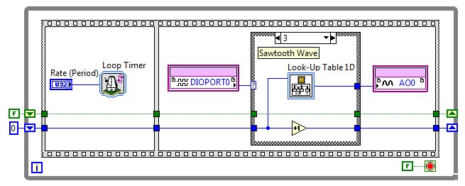
Figure 11d. Function Generator With R Series Case 3—Sawtooth Wave
The last case (Figure 11d) executes if both DIO 0 and DIO 1 are high, and this uses a look-up table to continuously generate a sawtooth wave. The look-up table VI is another Express VI with which you can store arbitrary waveform values and index through them programmatically. In this example, we’ve configured a sawtooth wave to be generated on analog output channel 0.
By storing all values on the FPGA, you eliminate the dependency of bus availability, as well as ensure hardware-timed speed and reliability on waveform updates. All of the triggering and synchronization flexibility described with analog input in earlier sections also applies to analog output; and with multifunction reconfigurable I/O devices, you can update different analog output channels at different rates, completely independent of each other. This means you can modify the frequency of a single periodic waveform without affecting the outputs of other channels. Keep in mind that this functionality is not possible on most data acquisition hardware.
Counter/Timer Operations
As mentioned earlier, typical multifunction DAQ devices have only four onboard counters, whereas multifunction reconfigurable I/O devices can implement counter functionality on any available digital line. Digital I/O nodes can take advantage of the specialized structure called the single-cycle Timed Loop in LabVIEW FPGA, with which you can execute code at specified rates ranging from 2.5 to 200 MHz. Using a 40 MHz clock, for example, you can use a single-cycle Timed Loop to create a 40 MHz counter on any digital line. Figure 12 (below) is an example of what the block diagram may look like.
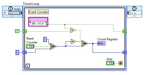
Figure 12. Simple Event Counter With R Series
Because the count value is sent to an indicator with a data type of U32 (32-bit integers), this code would produce a 40 MHz, 32-bit counter on the FPGA chip. You could copy and paste this several times to get multiple counters, all functioning on different digital lines completely parallel to one another. The real value with using multifunction reconfigurable I/O devices, however, is in the customization of counter operations. You can choose to increment the counter every three rising edges, or even trigger an analog acquisition based on the count register value. Many complex counter operations, such as finite pulse train generation or cascaded event counting require the use of two counters, which usually means all onboard counters for typical multifunction devices. With up to 160 digital lines, the maximum number of counters on reconfigurable hardware is rarely limited by I/O availability and is usually determined by the size of the FPGA chip. Because the LabVIEW code is running in silicon, there’s no need to “arm” or “rearm” general-purpose counters, and you get full control over counter operation.
Figure 13 (below) is an example of using counters to generate a continuous pulse train with a pause trigger in NI-DAQmx.
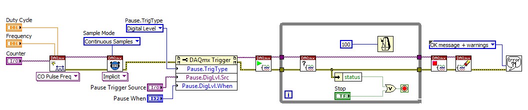
Figure 13. Continuous Pulse Train Generation and Pause Trigger With NI-DAQmx
In LabVIEW FPGA, the pause trigger needs no configuration, because a simple Case structure can implement the same functionality in silicon. Here’s what the same functionality looks like when implemented with a multifunction reconfigurable I/O device (Figure 14).
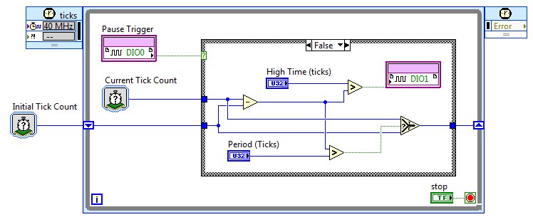
Figure 14. Continuous Pulse Train Generation and Pause Trigger With R Series
In this case, digital I/O line 0 is the Pause Trigger, and the pulse is generated on digital I/O line 1. The single-cycle Timed Loop is used to get 25 ns resolution on each pulse because that will be the value of a single tick using the 40 MHz timing source.
Data Transfer Methods
A major difference between traditional multifunction DAQ with the NI-DAQmx driver and reconfigurable hardware is the way that data transfer is implemented. The NI-DAQmx driver abstracts out all transfers from the device to the host computer. This must be completely programmed in LabVIEW for all FPGA-based hardware. There are several ways of buffering data onboard the device, and using different data transfer methods such as DMA channels and interrupt requests.
A FIFO buffer in LabVIEW FPGA is configured in the LabVIEW Project Explorer, and can be implemented using either onboard memory or hardware logic. Figure 18 shows how to configure a FIFO buffer of integer numbers in onboard block memory from the LabVIEW Project Explorer.
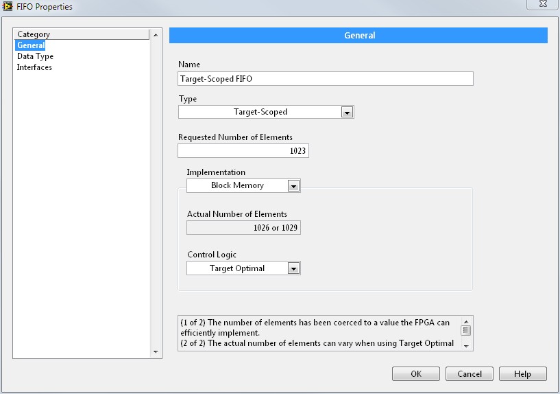
Figure 18. FIFO Configuration in LabVIEW FPGA
Once the FIFO is created, it can be used to transfer data between multiple loops on a LabVIEW FPGA block diagram. The example in Figure 19 shows data being written to the FIFO in the loop on the left, and then data being read from the FIFO in the loop on the right.
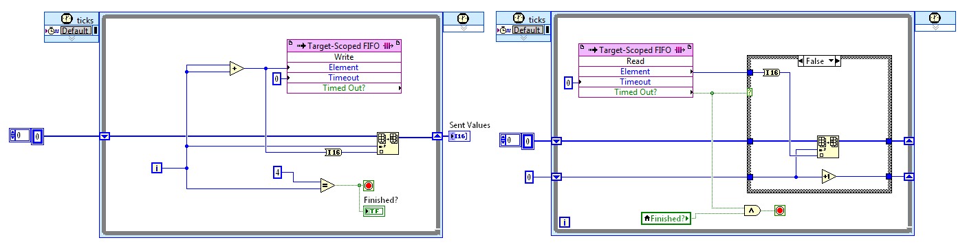
Figure 19. LabVIEW FPGA Block Diagram With FIFO and Multiple Loops
DMA channels, which are also implemented using LabVIEW FPGA FIFOs, are configured similarly in the LabVIEW Project Explorer.
Figure 20. DMA FIFO Configuration in LabVIEW FPGA
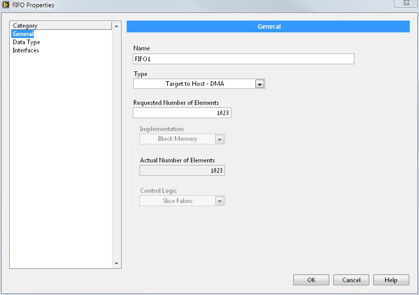
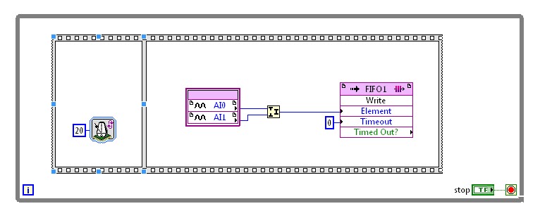
Figure 21. LabVIEW FPGA Block Diagram With DMA FIFO and Bit Packing
All DMA FIFO transfers are 32 bits, so when passing data from a 16-bit analog input channel, it’s often more efficient to combine samples and pass data two channels, or samples, at a time. This is known as bit-packing, which is shown in Figure 21. When data is passed directly to the host PC memory, it can then be read using the host interface functions on LabVIEW running in the Windows environment (Figure 22).
Figure 22. Host Interface Code With DMA FIFO Read and Bit Unpacking
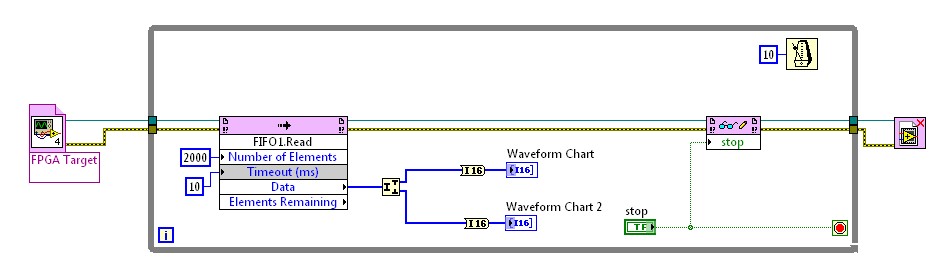
As shown in Figure 22, the host interface block diagram references the FPGA target VI and then continuously reads the DMA FIFO in a While Loop. The 32-bit data is split into the two 16-bit channels that were sampled and plotted on a waveform chart. The host interface VI can also read and write to any front panel indicator or control on the FPGA VI, and in this case the stop button control is being written to as well.
Conclusion
While fixed ASICs such as the NI-STC3 meet the majority of data acquisition requirements, complete flexibility and customization can be achieved only with the reconfigurable, FPGA-based I/O timing and control of R Series. With LabVIEW FPGA, triggering and synchronization tasks become as simple as graphically drawing the block diagram to do exactly what you need; and with independent analog and digital I/O lines, R Series boards can take advantage of the true parallelism that FPGAs offer. Whether it is multirate sampling, custom counter operation, or onboard decision making at 40 MHz, R Series devices have revolutionized the possibilities for multifunction data acquisition.