Importing HDL Code into FPGA VIs Using the HDL Interface Node
Overview
Contents
- Introduction
- Defining Ports
- Defining Functionality
- Using External HDL Code
- Emulating the HDL Interface Node
- Simulating the HDL Code
- Additional Resources
Introduction
You can use the LabVIEW FPGA Module to rapidly prototype and develop hardware in the same intuitive programming environment you use to develop software applications. However, you might have algorithms or applications in a hardware description language (HDL) that you want to use in FPGA VIs without rewriting the code in LabVIEW. If you have a block of HDL code you want to use in an FPGA VI, you can enter the code in the HDL Interface Node rather than rewriting the code in LabVIEW. You enter all the parameters and the HDL code in the Configure HDL Interface Node dialog box. The parameters become terminals on the HDL Interface Node. You then wire the parameters as you do any VI or function on the block diagram. Do not use the HDL Interface Node if you are not already familiar with an HDL programming language.
When you first place the HDL Interface Node on the block diagram of an FPGA VI, the node has no inputs, outputs, or defined functionality. Double-click the node to display the Configure HDL Interface Node dialog box. Use the Configure HDL Interface Node dialog box to configure inputs, outputs, internal functionality, external reference files, and so on. You can write HDL code to run in While Loops, single-cycle Timed Loops, or anywhere on the block diagram. You can configure the HDL Interface Node to use a separate emulation VI if you target an FPGA target emulator. You also can generate test benches to use in HDL simulators that test the functionality of the HDL component.
You cannot access I/O resources in the HDL code. If the HDL code needs to access I/O resources, you must create parameters for the input and output signals. You then can wire the parameters on the HDL Interface Node to FPGA Device I/O functions. In the FPGA Module 8.0, you can wire the parameters to the FPGA I/O functions.
Refer to the LabVIEW Help, which is available by selecting Help»Search the LabVIEW Help, for specific reference information about the HDL Interface Node and the Configure HDL Interface Node dialog box. Refer to the FPGA Module examples, available in NI Example Finder, for example VIs that use the HDL Interface Node.
Note LabVIEW currently supports VHDL in the HDL Interface Node. To use Verilog or another hardware design language, first compile the files to an EDIF or NGC netlist. You then can attach the netlist file to the HDL Interface Node on the External Files tab of the Configure HDL Interface Node dialog box and interface to the netlist file with HDL code on the Code tab.
Defining Ports
To interface the HDL code to the rest of the block diagram, you must define inputs and outputs for the HDL Interface Node. Begin configuring the HDL Interface Node by defining the parameters of the node on the Parameters tab of the Configure HDL Interface Node dialog box.
To configure a parameter, double-click a cell in the Name column of the Parameters table and enter the name of the parameter. The Name you enter corresponds to a port name in the HDL code. The Name appears as the parameter name on the terminal on the block diagram. Click the other cells to select the Direction, Type, and if the parameter is a Boolean array data type, the Length of the parameter. The HDL code for the parameter appears as a port in the hdlnode entity on the Code tab. You can use the Import from VI and Export to VI buttons on the Parameters tab to copy connector pane parameters between the HDL Interface Node and other VIs. You then can reuse the same inputs and outputs without defining each parameter more than once - once in the HDL Interface Node and once for each of the other VIs.
Note If you wire a Boolean array into an HDL Interface Node, element zero in the Boolean array maps to element n in the vector. The std_logic vector is described as n down to zero, where n is the number of elements - 1.
Defining Functionality
This section describes how to define the functionality of the HDL Interface Node using HDL code you enter directly into the HDL Interface Node. Enter the HDL code directly into the HDL Interface Node on the Code tab of the Configure HDL Interface Node dialog box. You can verify the syntax of the HDL code you enter by clicking the Check Syntax button.
Meeting the Requirements of Using the HDL Interface Node with the LabVIEW FPGA Module
LabVIEW and the LabVIEW FPGA Module follow a data flow model for running VIs. A block diagram node only executes when all its inputs are available. When a node completes execution, it supplies data to its output terminals and passes the output data to the next node in the data flow path. The HDL Interface Node uses an enable chain to follow the LabVIEW data flow model. The enable chain is the collection of signals and an associated protocol for controlling data flow of inputs and outputs of the HDL components. The HDL Interface Node includes the following execution control and enable chain signals as default ports, listed on the Code tab.
Execution Control Inputs
- clk—The clock signal supplied to the FPGA. For the LabVIEW FPGA Module, the clock signal is 40 MHz by default. You can use the clk input to clock the HDL code.
- reset—The signal asserted by LabVIEW at the beginning of execution, before the top-level VI runs or when you load the top-level VI from flash memory and run it. You can use the reset signal to initialize flip-flops in the HDL code that you want initialized when the VI runs. LabVIEW asserts the reset signal for at least one clock cycle.
Enable Chain Inputs
- enable_in—The signal LabVIEW asserts when all inputs wired to the HDL Interface Node are valid. LabVIEW asserts enable_in when all the nodes before the HDL Interface Node in the data flow finish executing. You can monitor enable_in to know when the HDL code can start executing.
- enable_clr—The signal the VI or loop asserts to indicate to the subVIs or nodes, including HDL Interface Nodes, in the VI or loop that they must deassert enable_out on the next rising edge of clk. In loops other than the single-cycle Timed Loop, enable_clr asserts after each loop iteration is complete and before the next iteration begins. If you use a single-cycle Timed Loop, the VI or loop does not assert enable_clr.
Enable Chain Output
- enable_out—Assert this signal in the HDL code when you want to indicate to the block diagram that the HDL code is complete and to signal to subsequent functions in the data flow to execute.
The HDL code you include in the FPGA VI must fit into LabVIEW data flow execution semantics by properly controlling the enable chain. If you do not properly control the enable chain, the HDL Interface Node might disrupt the execution of the other nodes on the block diagram.
Controlling Execution of the HDL Interface Node
You must control the execution of the HDL Interface Node differently depending on whether you place the node inside or outside a single-cycle Timed Loop on the block diagram. The single-cycle Timed Loop repeats the subdiagram inside it every clock cycle of the default FPGA clock until the conditional terminal, an input terminal, receives a particular Boolean value. LabVIEW can execute the subdiagram every clock cycle of the default FPGA clock because it removes the overhead of the enable chain for the LabVIEW functions.
Using the HDL Interface Node outside a Single-Cycle Timed Loop
If you do not use the HDL Interface Node in a single-cycle Timed Loop, select Single-Cycle Timed Loop Not Allowed on the Execution Control tab. LabVIEW asserts enable_in to signal that the inputs are valid and the HDL code can begin executing. Be sure to assert enable_out in the HDL code when the code has valid outputs and LabVIEW has asserted enable_in. Do not change the values of the outputs or enable_out until enable_clr asserts. After enable_clr asserts, you must deassert enable_out on the next rising edge of clk.
The following sequence occurs if you run an FPGA VI with a While Loop and an HDL Interface Node inside the While Loop on an FPGA target. The HDL code properly controls the enable chain.
- LabVIEW asserts reset to initialize the HDL code.
- The While Loop asserts enable_in to the HDL Interface Node, indicating the HDL code can begin executing.
- The HDL code receives enable_in, executes, makes sure outputs are valid and held constant, and asserts enable_out.
- The While Loop receives enable_out. When all the nodes in the While Loop complete, the While Loop checks the conditional terminal. If the While Loop runs again, the loop asserts enable_clr to all the nodes in the loop.
- The HDL code no longer needs to hold the outputs valid, so it deasserts enable_out one clock cycle later.
- The While Loop reasserts enable_in, and steps 3, 4, and 5 repeat.
The following timing diagram illustrates the previous sequence. The HDL code executes between the first and second rising edges of the Clock signal and between the fourth and fifth rising edges of the Clock signal.
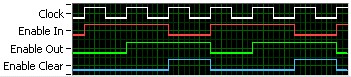
Figure 1: Example Timing Diagram.
The following VHDL code defines the enable chain for the component. The VHDL code also defines a simple adder you can use outside a single-cycle Timed Loop.
process( clk, reset )
begin
if( reset = '1' ) then
result <= (others=>'0');
enable_out <= '0';
elsif rising_edge(clk) then
result <= x + y; -- result and enable_out follow input by 1 clock cycle
if( enable_clr = '1' ) then
enable_out <= '0';
elsif( enable_in = '1' ) then
enable_out <= '1';
end if;
end if;
end process;
Using the HDL Interface Node inside a Single-Cycle Timed Loop
If you use the HDL Interface Node in a single-cycle Timed Loop, you must connect enable_out directly to enable_in and ignore enable_clr. For example, you could include enable_out <= enable_in;. All code in the HDL Interface Node executes every clock cycle.
The HDL Interface Node is easiest to use in the single-cycle Timed Loop if you use purely combinatorial logic in the HDL code and you do not register data internally in the HDL code. If you do register data internally for pipelining or storing state information, outputs from the HDL Interface Node might not be valid for the first few iterations of the loop.
The HDL code might need to store state information or pipeline the HDL code. If so, you can use enable_in as a clock enable for flip-flops. For example, you might have a design with an output based on an input of a previous iteration. Implement the design in the HDL code using flip-flops. An embedded shift register is equivalent to a flip-flop in hardware. The first one or more outputs from the HDL code to a terminal that come from an embedded shift register are invalid depending on the pipeline depth. An embedded shift register is equivalent to a bank of flip-flops in hardware.
If you know that only the first output is invalid but the second output is valid, place a checkmark in the Outputs Embed Shift Registers checkbox. When you use this checkbox, wire the output of the HDL Interface Node to an uninitialized LabVIEW shift register on right side of the single-cycle Timed Loop. Wire the left side of the shift register to the LabVIEW code. Typically, when a LabVIEW diagram is translated to HDL, LabVIEW replaces its own shift registers with flip-flops. However, when you place a checkmark in the Outputs Embed Shift Registers checkbox, LabVIEW does not replace the shift registers with flip-flops and instead relies on the flip-flops in the HDL code.
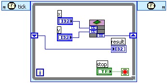
The following illustration demonstrates using the HDL Interface Node in a single-cycle Timed Loop and pipelining the result.
Figure 2: Pipelining the Results of the HDL Interface Node in a Single-Cycle Timed Loop.
The following VHDL code is included on the Code tab of the Configure HDL Interface Node dialog box.
process( clk, reset )
begin
if( reset = '1' ) then
result <= (others=>'0');
elsif rising_edge(clk) then
if enable_in = '1' then -- use enable_in as a clock enable
result <= x + y; -- result follows the inputs by one clock cycle
end if;
end if;
end process;
enable_out <= enable_in; -- drive the enable_out with enable_in
The VHDL code defines a simple adder that you can use inside a single-cycle Timed Loop. Notice that in this implementation, the VHDL code is pipelined to a depth of one and the result of the calculation is valid only after the first iteration of the single-cycle Timed Loop is complete. Also notice that the VHDL code includes a line to drive enable_out with enable_in.
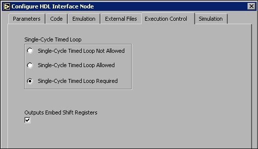
Because the output is registered, you can place a checkmark in the Outputs Embed Shift Registers checkbox on the Execution Control tab, as shown in the following figure, to indicate that the outputs must directly connect to uninitialized shift registers.
Figure 3: Execution Control Tab for VHDL with Registered Outputs and in a Single-Cycle Timed Loop.
Select Single-Cycle Timed Loop Required on the Execution Control tab of the Configure HDL Interface Node dialog box if you use the HDL Interface Node only in a single-cycle Timed Loop. The InSingleCycle generic appears in the hdlnode entity on the Code tab, though you do not need to use the InSingleCycle generic in the HDL code if you select Single-Cycle Timed Loop Required.
If you want to access physical I/O, use the ports on the HDL Interface Node. R Series targets have synchronization registers by default between the physical FPGA and the LabVIEW block diagram. If you want the HDL code to have direct access to the top-level FPGA pin, configure the number of synchronization registers as 0 on the I/O Synchronization tab of the FPGA Device I/O function Configure dialog box. The Digital Input function has two synchronization registers by default, and the Digital Output function has one synchronization register by default. In the FPGA Module 8.0, use the FPGA I/O Properties dialog box and FPGA I/O Node Properties dialog box to configure the number of synchronization registers. Refer to the LabVIEW Help, available by selecting Help»Search the LabVIEW Help in LabVIEW, for information about the FPGA Device I/O functions and I/O synchronization.
Using the HDL Interface Node Either inside a Single-Cycle Timed Loop or outside a Single-Cycle Timed Loop
Select Single-Cycle Timed Loop Allowed on the Execution Control tab to use the HDL Interface Node inside or outside a single-cycle Timed Loop. The InSingleCycle generic appears in the hdlnode entity on the Code tab. You must use the InSingleCycle generic in the HDL code and generate different code based on the value of the generic. Use the InSingleCycle generic to make sure only one of the two sections of HDL code executes for a particular instantiation of the HDL Interface Node. The following samples of VHDL code use the InSingleCycle generic and define a simple adder you can use inside or outside a single-cycle Timed Loop. The LabVIEW FPGA Module sets the value of the InSingleCycle generic during code generation. Only one of the blocks of code instantiates at a time based on the value of the InSingleCycle generic.
SingleCycleCode: -- if you use the HDL Interface Node in a single-cycle Timed Loop, use this code
if InSingleCycle generate
result <= x + y;
enable_out <= enable_in; -- drive the enable_out with enable_in
end generate;
NonSingleCycleCode: -- if you do not use the HDL Interface Node in a single-cycle Timed Loop, use this code
if not InSingleCycle generate
process( clk, reset )
begin
if( reset = '1' ) then
result <= (others=>'0');
enable_out <= '0';
elsif rising_edge(clk) then
result <= x + y; -- result and enable_out follow input by 1 clock cycle
if( enable_clr = '1' ) then
enable_out <= '0';
elsif( enable_in = '1' ) then
enable_out <= '1';
end if;
end if;
end process;
end generate;
The SingleCycleCode determines how the HDL Interface Node behaves when you place it in a single-cycle Timed Loop. The NonSingleCycleCode determines how the HDL Interface Node behaves when you do not place the node inside a single-cycle Timed Loop. Notice that the SingleCycleCode assigns enable_out to enable_in, and all the logic is combinatorial. Notice that the NonSingleCycleCode registers the output of the adder logic. The output then follows the input signals by one clock cycle. NonSingleCycleCode also places a one clock-cycle delay on the enable signal. Be sure to include code for each case if you select Single-Cycle Timed Loop Allowed.
Writing HDL Code to Adapt to Multiple Clock Rates
The HDL Interface Node includes a generic that allows different hardware implementations to be generated based on the value of the clock rate. The code for the ports and the generic appears in the hdlnode entity on the Code tab.
Use the ClockFrequency generic to generate statements in the HDL code based on the value of ClockFrequency. You can generate different HDL code based on the frequency you use to compile the design. For example, you might need a pulse to be 50 nanoseconds long. If the clock rate is 40 MHz, you generate a 2-cycle pulse. If the clock rate is 80 MHz, you generate a 4-cycle pulse. The following VHDL code demonstrates using the ClockFrequency generic to determine the pulse.
if ClockFrequency = 40000000
generate -- add code to generate 2-cycle pulse
end generate;
if ClockFrequency = 80000000
generate -- add code to generate 4-cycle pulse
end generate;
LabVIEW passes the actual value of the ClockFrequency generic to the HDL code when you compile the VI. Configure the default clock rate in the FPGA Target Options dialog box, which is available by selecting Target»Build Options in the Embedded Project Manager window. In the FPGA Module 8.0, configure the default clock rate in the FPGA Target Properties dialog box, which is available by right-clicking an FPGA target in the Project Explorer window and selecting Properties from the shortcut menu. You also can change the clock rate for a single-cycle Timed Loop within an FPGA VI by double-clicking the Input Node and selecting a clock rate in the Configure Timed Loop dialog box.
Using External HDL Code
You can define the functionality of the HDL Interface Node using HDL code in the implementation section of the Code tab in the Configure HDL Interface Node dialog box. However, you also might want to include external HDL code, such as external intellectual property, in the functionality of the HDL Interface Node. Use the External Files tab to reference external HDL code. You also can reference netlist files, such as EDIF files, or any other file used during the Xilinx compile process.
If you use external HDL code, you must include HDL code on the Code tab to interface with the external file. You also must have execution control and enable chain logic. You can place the execution control and enable chain logic on the Code tab, in the external file, or partially in both.
Click the Add File button to display the Add File dialog box. Browse to the file you want to add. You can add multiple external files. Click the Change Absolute/Relative button if the external files are in the same directory or a lower subdirectory as the FPGA VI where you use the HDL Interface Node and you want to use paths relative to the location of the FPGA VI.
Note: You must save the VI where you use the HDL Interface Node if you want to use a relative path.
Emulating the HDL Interface Node
You can test the logic of an FPGA VI before compiling it by targeting an FPGA target emulator. If you want the HDL Interface Node to execute when you target an FPGA target emulator, you must create an emulation VI and add it to the Configure HDL Interface Node dialog box. If you do not create an emulation VI, the HDL Interface Node executes as an empty VI while the rest of the block diagram executes normally.
To create an emulation VI, first be sure you have defined all the Parameters you need on the Parameters tab. Then click the Export to VI button. LabVIEW creates a template VI with the same terminals as the HDL Interface Node. You must write LabVIEW code in the new VI that emulates the HDL code and runs in Windows. If you add or remove a parameter from the HDL Interface Node, click the Export to VI button again and copy and paste the contents of the old emulation VI into the new emulation VI and rewire the block diagram and connector pane accordingly. Add the emulation VI to the HDL Interface Node on the Emulation tab.
Simulating the HDL Code
You can test the functionality of the HDL code using an HDL simulator. Click the Generate Enable Chain Testbench button on the Simulation tab of the Configure HDL Interface Node dialog box to generate the shell of a testbench. The testbench includes clk and enable_in. You must add code to the testbench shell to test the functionality you use in the HDL Interface Node. Click the Generate Single-Cycle Testbench button to generate the shell of a testbench that includes the additional code for using the HDL Interface Node in the single-cycle Timed Loop.