
Semiconductor Case Studies
Learn how engineers use NI hardware and software for researching and prototyping next-generation wireless technologies, validating or characterizing new silicon, or doing high-volume production test of semiconductor devices.
Wireless Research, Design, and Prototyping

Learn how researchers use NI software- defined radios to rapidly prototype wireless systems and new technologies like the FR3 frequency band, reconfigurable intelligent surface (RIS), integrated sensing and communications (ISAC or JCAS), and open RAN architectures.
Researchers created a modular platform with Python API and FPGA to test communication algorithms, RF hardware challenges, and to demonstrate concepts for 6G research.
Rutgers University uses NI Universal Software Radio Peripheral (USRP) transceivers for an open-ended, project-based course on wireless communications.
Rapidly prototype new wireless technologies with a high-performing testbed based on commercial off-the-shelf (COTS) software defined radios (SDR).
George Mason University built a test bed for Open RAN (O-RAN) architecture with NI SDR and standard interfaces provided by the Open AI Cellular (OAIC) platform.
Semiconductor Validation and Characterization
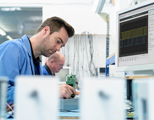
Discover how semiconductor engineers use NI hardware and software to accelerate design validation and IC characterization.
NewPath Research LLC developed a system for non-destructive, high-resolution carrier profiling with sub-nm resolution to support the semiconductor industry.
Holst Centre/imec created an automated test system to accurately verify and characterize new ultra-low-power semiconductor chip designs while saving time.
Melexis GmbH implemented a new validation test strategy to improve consistency, coverage, and analysis quality while decreasing time to market and improving quality.
Texas Instruments streamlined characterization of increasingly complex wireless and RF devices in a global design environment.
Dolphin Integration designed a modular solution to multiplex analog signals, generate and acquire analog and digital signals, and control components using I²C bus.
Infineon Technologies created an unmanned test bench with an intuitive user interface for integrating and automating a complete microcontroller testing workflow.
NXP Semiconductors fulfilled automated testing of peripheral software without sizeable investment into specialized test hardware infrastructure or constant upgrading.
Texas Instruments reduced cost, measurement, and characterization time while improving quality for RFIC test and development with NI PXI instruments.
Texas Instruments built an automated test system that supports test sequencing across hundreds of PMICs and interacts with multiple instruments, SMUs, and more.
Qualcomm Atheros improved WLAN test speeds by more than 200 times compared to traditional rack-and-stack instruments while significantly improving test coverage.
ST-Ericsson upgraded a characterization lab with a validation test solution that meets a variety of RF standards for semiconductor chip tests and reduces test times.
Cypress Semiconductor Technology India Pvt. Ltd developed an ATE-like platform called CyMatrix to reduce bench characterization of system-on-chip (SoC) products.
Soliton Technologies Pvt. Ltd. developed a semiconductor framework to increase automaton and facilitate accelerated product development and validation cycles.
Researchers developed a system for scanning electron microscope (SEM) control and built a .NET interoperability assembly to communicate with external applications.
High-Volume Semiconductor Production Test

Learn how engineers used NI high-volume manufacturing test solutions and advanced analytics to improve semiconductor yield and quality.
Amfax developed an XYZ measurement-based inspection technology to help companies improve the quality of their manufactured PCB assemblies.
Researchers utilized NI SourceAdapt technology to make an LED tester five times faster than others composed of a traditional rack-and-stack source measure unit (SMU).
imec used electrical wafer-level tests to detect process-related issues at an early stage to manage yield drops, optimize the process flow, reduce costs, and decrease time to market.
Jetek Technology developed 32-site microelectromechanical sensors (MEMS) microphone test equipment, that meets industry standards, in a short period of time.
imec vzw developed an automated system to characterize prototype probe cards for large-array, fine-pitch microbumps on advanced test wafers using the STS.
ON Semiconductor Belgium developed a high-end, scalable, and cost-effective mixed-signal ATE production tester that enables wafer sort and final test for image sensors.
Afore enabled testing of low‑g accelerometers and gyroscopes with the Afore KRONOS wafer-level test handler and integrated PXI-based hardware.
SYNERGIE CAD INSTRUMENTS developed FlexyTest; a versatile solution that maximizes test fixtures and extends their operating life without affecting ATE productivity.
Researchers created a custom test executive to quickly assemble and configure new custom test sequences for hybrid semiconductor component production testing.
Project Integration LLC created an automated test system to measure the parameters of high-power IGBT and MOSFET transistors with an intuitive user interface.
G Systems, LP developed a system to increase wafer probe test throughput and improve tester flexibility for use with various semiconductor sensors.
ST-Ericsson created a real-time system to localize failure mechanisms causing abnormal electrical behavior in ICs.
Researchers created a system for simultaneous tests of up to four sensors, resulting in 6X reduction in test time from the previous-generation test system.