Understanding the PXIe-4081 7½-Digit FlexDMM Architecture
Contents
- Overview
- Traditional DMM Limitations
- National Instruments FlexDMM Technology
- Low-Noise, High-Stability Front-End Architecture
- Self-Calibration
- Voltage Measurement Architecture
- Current Measurement Architecture
- 1.8 MS/s Isolated Digitizer Architecture
- Resistance Measurement Architecture
- Conclusion
Overview
NI introduced its first PXI FlexDMM in 2002. This product provided engineers with a solution to the measurement challenges inherent in traditional precision instruments—limited measurement throughput and flexibility. The FlexDMM helped overcome these challenges by delivering measurement throughput rivaling higher-resolution digital multimeters (DMMs) which often cost thousands of dollars more. NI has continued to innovate on the FlexDMM architecture since the release by:
- Doubling the throughput of its fastest measurement mode
- Adding a 1.8 MS/s isolated, high-voltage digitizer mode
- Releasing a PCI version of the PXI-4070
- Releasing the PXIe-4082 6½-digit FlexDMM and LCR meter
The latest innovation is the NI PXIe-4081 7½-digit FlexDMM. The PXIe-4081 FlexDMM offers 26 bits of accuracy and resolution, which provides 10 times more resolution and up to 60 percent more accuracy than the previous FlexDMM devices. The PXIe-4081 also offers extremely wide measurement ranges, as shown in Table 1, so you can measure DC voltage from ±10 nV to 1000 V, current from ±1 pA to 3 A, and resistance from 10 µΩ to 5 GΩ, as well as take frequency/period and diode measurements. The FlexDMM features an isolated digitizer mode, in which you can acquire DC-coupled waveforms at sample rates up to 1.8 MS/s at all voltage and current modes. This document provides a detailed comparison of the FlexDMM and traditional DMM analog-to-digital converters (ADCs) and architectures.
PXIe-4081
| PXIe-4080/4082
| |
| Max Resolution | 7½ digits (26 bits)
| 7 digits (23 bits)
|
| Voltage Ranges | ||
| Maximum DC | 1000 V
| 300 V
|
| DC sensitivity | 10 nV
| 100 nV
|
| Maximum AC rms (peak) | 700 Vrms (1000 V)
| 300 Vrms (425 V)
|
| Common mode voltage | 500 V
| 300 V
|
| Current Ranges | ||
| Maximum DC | 3 A
| 1 A
|
| DC sensitivity | 1 pA
| 10 nA
|
| Maximum AC rms (peak) | 3 A (4.2 A)
| 1 A (2 A)
|
| AC rms sensitivity | 100 pA
| 10 nA
|
| Resistance Ranges | ||
| Maximum | 5 GΩ
| 100 MΩ
|
| Sensitivity | 10 µΩ
| 100 µΩ
|
| LCR Ranges1 | ||
| Capacitance | N/A
| 0.05 pF to 10,000 µF
|
| Inductance | N/A
| 1 nH to 5 H
|
| Cost | $3,690 USD
| $2,406/$3,209 USD
|
Table 1. FlexDMM Input Comparison
1 PXIe-4082 only. Consider the PXI LCR Meter for other options for measuring inductance and capacitance.
Traditional DMM Limitations
Traditional DMMs generally focus on resolution and precision and do not offer high-speed acquisition capability. There is some inherent limitation in noise performance versus speed, of course, which is a function of basic physics. The Johnson thermal noise of a resistor is an example of one theoretical limit, and semiconductor device technology sets some practical limitations. But you have many other options to help you achieve the highest possible measurement performance.
Some specialized high-resolution DMMs tease with both resolution and somewhat higher speeds, but they are very expensive – near $8,000 USD – and available only in full-rack configurations that consume significant system or bench space.
Another DMM speed limitation is driven by the traditional hardware platform – the GPIB (IEEE 488) interface bus. This interface, in use since the 1970s, is often considered the standard despite trade-offs in speed, flexibility, and cost. Most traditional “box” DMMs use this interface, although alternative interface standards, such as USB and Ethernet, are now available as options with traditional DMMs. All of these interfaces communicate with the DMM by sending messages to the instrument and waiting for a response, which is inherently slower than the register-based access used in PXI modular instruments.
Even with the first attempts to move away from the GPIB interface, the basic limitation with DMMs in both speed and precision continues to be the ADCs used in these products. To better understand the technologies used, you need to examine more closely what they offer in terms of performance.
Dual-Slope ADC Technology
From a historic perspective, one of the oldest but most common forms of precision A/D conversion is the Dual-Slope ADC. This technique has been widely used since the 1950s. It is essentially a two-step process. First, an input voltage (representing the signal to be measured) is converted to a current and applied to the input of an integrator through switch S1. When the integrator is connected to the input (at the beginning of the integration cycle or aperture), the integrator ramps up until the end of the integration cycle or aperture, at which time the input is disconnected from the integrator. Now, a precision, known reference current is connected to the integrator through switch S2 and the integrator is ramped down until it crosses zero. During this time, a high-resolution counter measures the time it takes for the integrator to ramp down from where it started. This measured time, relative to the integration time and reference, is proportional to the amplitude of the input signal. See Figure 1.
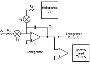
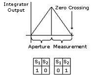
Figure 1. Dual-Slope Converter Block Diagram
This technique is used in many high-resolution DMMs, even today. It has the advantage of simplicity and precision. With long integration times, you can increase resolution to theoretical limits. However, the following design limitations ultimately affect product performance:
- Dielectric absorption of the integrator capacitor must be compensated, even with high-quality integrator capacitors, which can require complicated calibration procedures.
- The signal must be gated on and off, as must the reference. This process can introduce charge injection into the input signal. Charge injection can cause input-dependent errors (nonlinearity), which are difficult to compensate for at very high resolutions (6½ digits or more).
- The ramp-down time seriously degrades the speed of measurement. The faster the ramp down, the greater the errors introduced by comparator delays, charge injection, and so on.
Some topologies use a transconductance stage prior to the integrator to convert the voltage to a current, and then use “current steering” networks to minimize charge injection. Unfortunately, this added stage introduces complexity and possible errors.
Despite these design limitations, dual-slope converters have been used in a myriad of DMMs from the most common bench or field service tools to high-precision, metrology-grade, high-resolution DMMs. As with most integrating A/D techniques, they have the advantage of providing fairly good noise rejection. Setting the integration period to a multiple of 1/PLC (power line frequency) causes the A/D to reject line frequency noise – a desirable result.
Charge-Balance-with-Ramp-Down ADC Technology
Many manufacturers overcome the dielectric absorption and speed problems inherent in dual-slope converters by using the charge-balance-with-ramp-down A/D technique. This technique is fundamentally similar to the dual slope but applies the reference signal in quantized increments during the integration cycle. This is sometimes called “modulation.” Each increment represents a fixed number of final counts. See Figure 2.
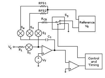
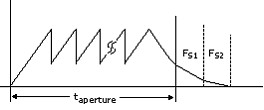
Figure 2. Charge-Balance Converter Block Diagram
During this integration phase, represented in Figure 2 by taperture, S1 is turned on and Vx is applied through R1, which starts the integrator ramping. Opposing current is applied at regular intervals through switches, S2 and S3. This “balances” the charge on C1. Measurement counts are generated each time S5 is connected to VR. In fact, for higher-resolution measurements (longer integration times), most of the counts are generated during this taperture phase. At the end of the charge-balance phase, a precision reference current is applied to the integrator, as is done in the case of the dual-slope converter. The integrator is thus ramped down until it crosses zero. The measurement is calculated from the counts accumulated during the integration and added to the weighted counts accumulated during the ramp down. Manufacturers use two or more ramp-down references, resulting in fast ramp downs to optimize speed and then slower “final slopes” for precision.
Although you can greatly improve your integrator capacitor dielectric absorption problems with the charge-balance with ramp-down A/D, it has performance benefits similar to the dual-slope converter. (In fact, some dual-slope converters use multiple ramp-down slopes.) Speed is greatly improved because the number of counts generated during the charge- balance phase reduces the significance of any ramp-down error, so ramp down can be much faster. However, there is still significant dead time if you make multiple measurements or if you digitize a signal because of disarming and rearming the integrator.
This type of ADC, in commercial use since the 1970s, has evolved significantly. Early versions used a modulator similar to that of a voltage-to-frequency converter. They suffered from linearity problems brought on by frequency-dependent parasitic effects and were thus limited in conversion speed. In the mid-1980s the technique was refined to incorporate a “constant frequency” modulator, which is still widely used today. This dramatically improved both the ultimate performance and manufacturability of these converters.
Sigma-Delta Converter Technology
Sigma-delta converters, or noise-shaping ADCs, have historic roots in telecommunications. Today, the technique is largely used as the basis for commercially available off-the-shelf A/D building blocks produced by several manufacturers. Significant evolution has taken place in this arena over the last decade (driven by a growing need for high dynamic range conversion in audio and telecommunications), and much research is still ongoing. Some modular DMMs (PXI(e), PCI(e), and VXI) use sigma-delta ADCs at the heart of the acquisition engine today. They are also commonly used to digitize signals for:
- Dynamic signal analysis (DSA)
- Commercial and consumer audio and speech
- Physical parameters such as vibration, strain, and temperature, where moderate-bandwidth digitizing is sufficient
A basic diagram of a sigma-delta converter is shown in Figure 3.
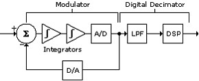
Figure 3. Sigma-Delta Converter Block Diagram
The basic building blocks of a sigma-delta converter are the integrator or integrators, one-bit ADC and DAC (digital-to-analog converter), and digital filter. You conduct noise shaping by combining the integrator stages and digital filter design. You have numerous techniques for implementing these blocks. Different philosophies exist regarding the optimum number of integrator stages, number of digital filter stages, number of bits in the A/D and D/A converters, and so on. However, the basic operational building blocks remain fundamentally the same. A modulator consisting of a one-bit charge-balancing feedback loop is similar to that described above. The one-bit ADC, because of its inherent precision and monotonicity, leads the way to very good linearity.
There are many advantages to using commercially available sigma-delta converters:
- They are fairly linear and offer good differential nonlinearity (DNL)
- You can control signal noise very effectively
- They are inherently self-sampling and tracking (no sample-and-hold circuitry required)
- They are generally low in cost
However, there are some limitations to using off-the-shelf sigma-delta ADCs in high-resolution DMMs:
- Speed limitations, especially in scanning applications, due to pipeline delays through the digital filter
- Although generally linear and low noise, manufacturer specifications limit precision to 5½ digits (19 bits)
- Modulation “tones” can alias into the passband, creating problems at high resolutions
- Limited control over speed-noise trade-offs, acquisition time, and so on
National Instruments FlexDMM Technology
The FlexADC is the backbone of the NI FlexDMM family (PXIe-4080, PXIe-4081, PXIe-4082). The FlexADC provides the noise, linearity, speed, and flexibility required to achieve high-speed, high-precision measurements. The FlexADC, shown in Figure 4, is based on a combination of off-the-shelf high-speed ADC technology and a custom-designed sigma-delta converter. This combination optimizes linearity and noise for up to 7½-digit precision and stability yet offers digitizer sampling rates up to 1.8 MS/s.
Figure 4. FlexADC Converter
The block diagram in Figure 4 shows a simplified model of how the FlexADC operates. At low speeds, the circuit exploits the advantages of the sigma-delta converter. The feedback DAC is designed for extremely low noise and exceptional linearity. The lowpass filter provides the noise shaping necessary for effective performance across all resolutions. No ramp down is needed because the ultrahigh-precision 1.8 MS/s modulator provides extremely high-resolution conversion without it. At high speeds, the 1.8 MS/s modulator combines with the fast-sampling ADC to provide continuous-sample digitizing. The digital signal processor (DSP) provides real-time sequencing, calibration, linearization, AC true-rms computing, decimation, as well as the weighted noise filtering used for the DC functions.
The FlexADC has several advantages:
- The unique architecture of the FlexDMM offers a continuously variable reading rate from 7 S/s at 7½ digits to 10 kS/s at 4½ digits, as shown in Figure 5.
- You can operate the FlexADC as a digitizer with a sampling rate up to 1.8 MS/s.
- Because of the custom sigma-delta modulator, noise shaping and digital filtering have been optimized for use in DMM and digitizer applications.
- Unlike in other ADC conversion techniques, it is not necessary to turn the input signal on and off. Therefore, you can achieve continuous, contiguous signal acquisition.
- You can accomplish direct ACV conversion and frequency response calibration without the use of a conventional analog AC Trms converter and analog “trimmers” for flatness correction.
- You can dramatically reduce input signal noise on all functions with appropriate noise-shaping algorithms (see DC Noise Rejection).
- You can implement advanced host-based functions with NI LabVIEW software once you digitize the signals, leading to an almost endless list of signal characterization options (fast Fourier transform, calculating impedances, AC crest factor, peak, AC average, and so on).
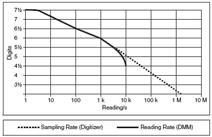
Figure 5. FlexDMM DC Reading Rates
Table 2 compares all four of these ADC architectures.
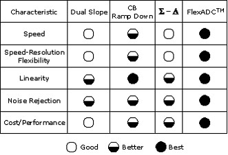
Table 2. ADC Architecture Comparison
Low-Noise, High-Stability Front-End Architecture
All FlexDMMs feature some of the most stable onboard references available. As a voltage reference, the FlexDMM uses a well-known selected thermally stabilized reference that provides unmatched performance on the market. The result is a maximum reference temperature coefficient of less than 0.3 ppm/ºC. The time stability of this device is on the order of 8 ppm/year. No other DMM in this price range offers this reference source and its accompanying stability. That is why the FlexDMM offers a two-year accuracy guarantee.
Resistance functions are referenced to a single 10 kΩ highly stabilized metal-foil resistor originally designed for demanding aerospace applications. This component has a guaranteed temperature coefficient of less than 0.8 ppm/ºC and a time stability of less than 25 ppm/year.
Solid-State Input Signal Conditioning
A major source of measurement error in most traditional DMMs is electromechanical relay switching. Contact-induced thermal voltage offsets can cause instability and drift. FlexDMM devices eliminate all but one relay in the DCV, ACV, and resistance path. A special relay-contact configuration cancels the thermal errors in this single relay. This relay is switched only during self-calibration. All measurement-related switching for function and range changing is done with low-thermal, highly reliable solid-state switching. Thus, electromechanical relay wear-out failures are all but eliminated. Figure 6 shows an overnight drift performance of the most sensitive range, the 100 mV range. Each division is 500 nV. For comparison, the same measurement made under identical conditions with a traditional 6½-digit DMM and a full-rack 8½-digit DMM is shown in Figure 6.
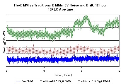
Figure 6. Curve Showing FlexDMM (lower) 100 mV Range Stability with Shorted Input, Compared to a Traditional DMM (upper) – 500 nV/Division
Linearity
Linearity is a measure of the “quality” of a DMM transfer function. It’s important in conversion-component characterization applications to offer DNL and INL (integral nonlinearity) performance substantially better than that available in off-the-shelf ADCs. The FlexADC is designed for excellent linearity, both DNL and INL. Linearity is also important because it determines the repeatability of the self-calibration function. The Figure 7 plot shows a typical FlexDMM linearity plot measured on the 10 V range from -10 to +10 V.
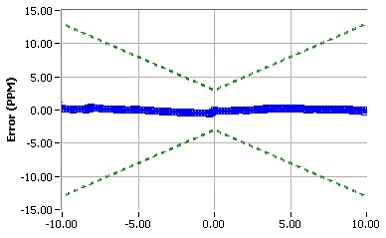
Figure 7. 10 VDC Range Linearity
Self-Calibration
Traditional 6½- and 7½-digit DMMs are calibrated at a particular temperature, and this calibration is characterized and specified over a limited temperature range, usually ±5 ºC (or even ±1 ºC in some cases). Thus, whenever the DMM is used outside of this temperature range, its accuracy specifications must be derated by a temperature coefficient, usually on the order of 10 percent of the accuracy specification/ºC. So at 10 ºC outside of this specified range, you may have twice the specified measurement error, which can be a serious concern when absolute accuracy is important.
If the excursions in temperature exceed these limits and tight specifications are required, then recalibration is also required at the new temperature. Take, for example, the 10 VDC range on traditional 7½-digit DMMs. A DMM may have an accuracy of the following:
Two-year accuracy: (12 ppm of reading + 0.5 ppm of range) for T = ±5 ºC of Tselfcal
With this specification, if you apply 5 V to the input programmed to read a 10 V range, the error is:
12 ppm of 5 V + 0.5 ppm of 10 V = 10 µV, for the temperature range determined by the temperature at the last self-calibration.
Assuring PPM-Level Precision
To mitigate errors caused by these effects, all FlexDMM devices incorporate a proprietary self-calibration function for volts direct current (VDC), resistance, diode, and digitizer mode. This function is significant for the following reasons:
1. The self-calibration function corrects for all signal-path gain and offset errors within the DMM back to the precision, high-stability internal voltage reference previously described.
2. Self-calibration accounts for all resistance current source, gain, and offset errors. In resistance, all errors are corrected back to the single internal 10 kW precision resistor.
3. Self-calibration takes one minute and fully recalibrates all ranges of voltage, resistance, and digitizer functions. In traditional DMMs, more than 10 minutes are required to perform this function.
The result is a highly accurate, ultrastable DMM at any operating temperature, well outside of the traditional 18 to 28 ºC, with the use of self-calibration. For the example above, the additional error introduced by the temperature coefficient using self-calibration would be fully covered in the 90-day and two-year specifications and would be:
tempco = (0.3 ppm of reading + 0.01 ppm of range)/ºC, then the additional error is:
22 ºC x tempco = (6.6 ppm of reading + .22 ppm of range) or 35.2 µV total uncertainty. This error at 50 ºC ambient temperature is almost four times worse than the specified one-year accuracy.
This represents an enormous improvement in accuracy over the full operating temperature range of the FlexDMM. Table 3 summarizes these results.
|
Condition
|
Traditional 7½-Digit DMM (1-Year)
|
PXI-4071 7½-Digit FlexDMM
(2-Year) |
| Measurement within 18 to 28 ºC |
160 µV
|
65 µV
|
| Measurement at 50 ºC without Self-Calibration |
600 µV
|
111 µV
|
| Measurement at 50 ºC with Self-Calibration |
600 µV (no self-calibration available)
|
80 µV
|
Table 3. Example Summary – Uncertainty Analysis, Measuring 5 V on 10 V Range
Note that using the FlexDMM with self-calibration provides accuracy at 50 ºC, which is more than seven times better than traditional methods. Table 4 compares self-calibration to the traditional “Factory” calibration.
|
Calibration Option
|
Application
|
When
|
Performance Benefit
|
| “Factory” Calibration |
Recalibrate time drift of
onboard references Corrects for AC flatness drift for all functions |
Every 2 years
|
To full specifications
|
| Self-Calibration |
7½-digit precision –
recalibrates measurement path and ADC for VDC, resistance, diode, and digitizer |
90 days or for temperature change >1 ºC
|
To specifications on VDC, resistance, diode, and digitizer functions over FULL operating temperature range
|
Table 4. Calibration Comparison
Voltage Measurement Architecture
No compromise was made in offering high-stability, metrology-class DC and AC voltage function. Several factors contribute to the FlexDMM achieving this performance:
- The availability and quality of miniature surface-mount, high-performance, precision components has improved dramatically over the last 10 years
- Smaller, tightly laid out electronic packaging actually improves performance, especially thermal tracking between precision components
- The use of the FlexADC and DSP for ACV computation and frequency response calibration simplifies input signal conditioning into a common path, reducing components, complexity, and switching
- The lack of a “Front-Rear” switch (common in box DMMs) simplifies the input layout, reduces critical circuit signal path resistance, and improves signal integrity
- The power supply, a common component in a PXI system chassis, does not consume space on the measurement module
High-Voltage Architecture
With the NI PXI-4071, you can measure 1000 VDC and 700 VAC Trms at CAT I levels. To accurately measure 1000 V in an ultrasmall PXI module, you must consider component breakdown, voltage spacing, attenuator designs, and power dissipation limitations in the front-end circuitry.
Single 10 MΩ Input Attenuator
Traditionally, DMMs use both 1 MΩ and 10 MΩ attenuators in their front-end signal conditioning circuits. A 1 MΩ attenuator, when used to provide the signal conditioning for a 700 VAC signal, dissipates more than 0.5 W. This is a difficult requirement for a miniature precision component. Controlling temperature-coefficient-induced errors is a challenge even for a physically large component. Hence, eliminating the need for the 1 MΩ attenuator is required. Another important reason why 1 MΩ attenuators are used in traditional DMMs is the wide AC bandwidth. Traditional 10 MΩ attenuator designs cannot attain the same level of AC bandwidth achieved by 1 MΩ attenuator designs.
The PXIe-4081 FlexDMM incorporates an innovative scaled bootstrap design to null the attenuator capacitance that traditionally impedes wide bandwidth performance. This bootstrap, shown in Figure 8, is designed and carefully laid out to minimize stray capacitance loading the 100 kΩ attenuator leg of the input attenuator network RN. With the addition of the scaled bootstrap formed by R1-R4, C1, and U1, flat step response is assured. Most importantly, the characteristic response achieved is very close to that of a single pole RC, which is important for digitizer and DC step response.
Figure 8. PXI-4071 Scaled Bootstrap
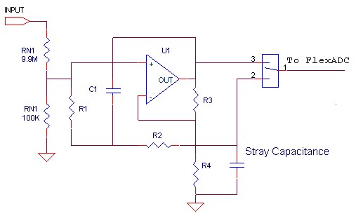
Secondly, the PXIe-4081 uses the digital AC DSP flatness correction to compensate the residual attenuator flatness without the use of compensation capacitors. These two compensation techniques deliver an order of magnitude improvement over what would otherwise be possible given the requirement that the single attenuator be capable of passing ACrms, precision DC, and digitizer signals.
Component Breakdown and Voltage Spacing
One of the most daunting enemies to high-voltage measurement is range selection switch (relay) breakdown. Traditionally, DMMs use high-voltage relays. High-voltage relay switching and high reliability are not easy to achieve together in any package, let alone a miniaturized one.
To meet both of these requirements, the PXIe-4081 implements a novel new solid-state device for range selection capable of withstanding well over 1000 V in the off state. This device has none of the traditional reliability problems of electromechanical relays because there are no contacts to be damaged by high-voltage switching, and no contact life limitations. The secondary benefit of solid-state input signal conditioning is excellent low-level DC thermal performance, an unheard of combination in any 1000 V DMM presently available for less than $5,000 USD.
By moving to solid-state high-voltage switching, eliminating the need for a 1 MOhm divider, and using DSP to eliminate calibration components, you can meet voltage spacing requirements with the increased availability of board surface and bulk area. You can now adjust the layout to meet the CAT I requirements for 1000 V PXI instrumentation.
DC Noise Rejection
DC noise rejection is an exclusive NI feature available for DC measurements on all FlexDMM devices. Each DC reading returned by the FlexDMM is actually the mathematical result of multiple high-speed samples. By adjusting the relative weighting of those samples, you can adjust the sensitivity to different interfering frequencies. Three different weightings are available – normal, second-order, and high-order.
Normal
When you select normal DC noise rejection, all samples are weighted equally. This process emulates the behavior of most traditional DMMs, providing good rejection of frequencies at multiples of f0 where f0 = 1/taperture , the aperture time selected for the measurement. Figure 9 illustrates normal weighting and the resulting noise rejection as a function of frequency. Notice that good rejection is obtained only very near multiples of f0.
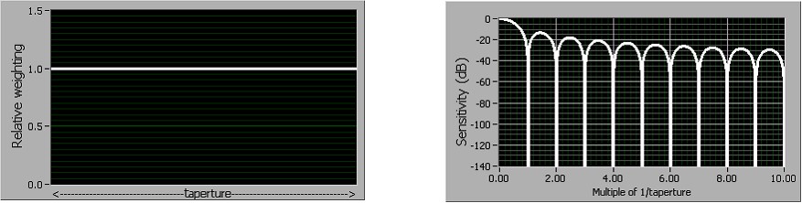
Figure 9. Normal DC Noise Rejection
Second-Order
Second-order DC noise rejection applies a triangular weighting to the measurement samples, as shown in Figure 10. Notice that very good rejection is obtained near even multiples of f0, and that rejection increases more rapidly with frequency than with normal sample weighting. Also notice that the response notches are wider than they are with normal weighting, resulting in less sensitivity to slight variations in noise frequency. You can use second-order DC noise rejection if you need better power line noise rejection than you can get with normal DC noise rejection but you can’t afford to sample slowly enough to take advantage of high-order noise rejection. For example, you can set the aperture to 33.333 ms for a 60 Hz power line frequency.
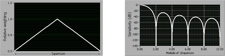
Figure 10. Second-Order DC Noise Rejection
High-Order
Figure 11 illustrates high-order sample weighting and its resulting noise rejection as a function of frequency. Notice that noise rejection is good starting around 4f0 and is excellent above 4.5f0. Using high-order DC noise rejection, you achieve almost no sensitivity to noise at any frequency above 4.6f0. A FlexDMM using high-order DC noise rejection with a 100 ms aperture (10 readings/s) can deliver full 6½-digit accuracy with more than 1 V of interfering power-line noise on the 10 V range at any frequency above 46 Hz. This is the equivalent of >110 dB normal mode rejection, insensitive to variations in power-line frequency.
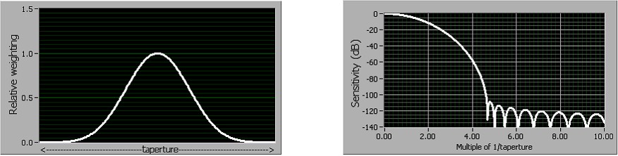
Figure 11. High-Order DC Noise Rejection
Table 5 summarizes the differences between the three DC noise rejection settings.
| DC Noise Rejection Setting | Lowest Frequency for Noise Rejection | High-Frequency Noise Rejection |
| Normal | 1/taperture | Good |
| Second-order | 2/taperture | Better |
| High-order | 4/taperture | Best >110 dB rejection |
Table 5. DC Noise Rejection Settings
AC Voltage Measurements
AC signals are typically characterized by rms amplitude, which is a measure of their total energy. RMS stands for root-mean-square; to compute the rms value of a waveform, you must take the square root of the mean value of the square of the signal level. Although most DMMs do this nonlinear signal processing in the analog domain, the FlexDMM uses an onboard DSP to compute the rms value from digitized samples of the AC waveform. The result is quiet, accurate, and fast-settling AC readings. The digital algorithm automatically rejects the DC component of the signal, making it possible to bypass the slow-settling input capacitor. To measure small AC voltages in the presence of large DC offsets, such as ripple on a DC power supply, the FlexDMM offers the standard AC volts mode, in which the coupling capacitor eliminates the offset and the FlexDMM uses the most sensitive range.
The rms algorithm used by the FlexDMM requires only four periods (cycles) of the waveform to obtain a quiet reading. For example, it requires a measurement aperture of 4 ms to accurately measure a 1 kHz sine wave. The advantage brought about by this technique extends to system performance. With traditional DMMs, it is necessary to wait for an analog Trms converter to settle before you make a measurement. With the FlexDMM, there is no Trms converter to settle. The result is faster AC reading rates, and this advantage is realized in systems with switching.
The digital approach to rms computation offers accuracy benefits as well. The algorithm is completely insensitive to crest factor, and can deliver exceptionally quiet and stable readings. The FlexDMM guarantees AC accuracy down to 1 percent of full-scale, rather than the 10 percent of full-scale offered by traditional DMMs, and usable readings are obtainable even below 0.1 percent of full-scale.
Current Measurement Architecture
Extending DMM current measurement dynamic range is a requirement to meet growing customer demand. On the upper end, you may need to monitor battery, circuit, or electromechanical device load performance. Today’s integrated electronic devices require more power. Thus, the need to test or characterize these devices at levels greater than 1 A is increasing. On the lower end, many applications today such as semiconductor device “off” characteristics may have microampere or nanoampere levels.
The PXIe-4081 addresses both needs by implementing a novel solid-state current measurement configuration that provides eight DC current ranges from 1 µA to 3 A and six ACrms current ranges from 100 µA to 3 A. The 1 µA range offers sensitivity down to 1 pA, or 10-12 A. Providing both extremes requires a unique circuit design approach. The challenges of high-voltage or current-overload protection and low-leakage measurement have historically been mutually exclusive. The FlexDMM implements a unique design approach, diagrammed in Figure 12. This greatly simplified figure shows three of the five current ranges used in the PXI-4071.
Figure 12. Simplified PXI-4071 Current Signal Conditioning
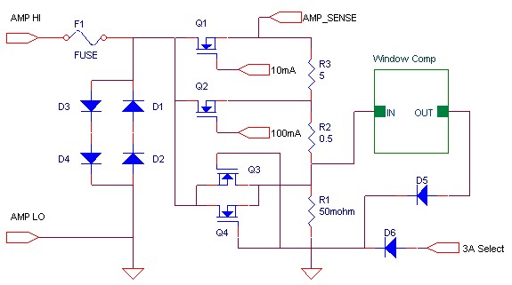
Using solid-state devices throughout for current range selection achieves higher reliability and improved protection in a small physical space. In addition, two of the current range selection devices – Q3 and Q4 – actually come into play during overloads, thus protecting the high-stability current-sensing resistors and providing robustness for the most demanding applications.
1.8 MS/s Isolated Digitizer Architecture
The PXIe-4081 FlexDMM also has the capability to acquire DC-coupled waveforms up to 1000 VDC and 700 VAC (1000 Vp) input at a maximum sampling rate of 1.8 MS/s. You can vary the digitizer resolution from 10 to 26 bits by simply changing the sampling rate. With the isolated digitizer capability, the FlexDMM can minimize overall test system cost by eliminating the need to purchase a separate digitizer and reducing the test fixture size and maintenance costs.
By combining LabVIEW graphical development software with the isolated digitizer mode of the FlexDMM, you can analyze transients and other nonrepetitive high-voltage AC waveforms in both the time and frequency domains. No other high-resolution DMM features this capability.
For example, a common application in the automotive industry is the measurement of the flyback voltage on an ignition coil. The ignition coil, which creates the high voltages used to drive the spark plugs in the engine, is made up of a primary coil and a secondary coil. The secondary coil generally has many more turns of wire than the primary coil because the turns ratio times the voltage applied to the primary coil determines the output voltage. When the current is suddenly commutated off, the collapse of the magnetic field induces a large voltage (+20,000 V) onto the secondary coil. This voltage is then routed to the spark plugs.
Because the voltages are so high on the secondary coil, tests are actually made on the primary coil. The flyback waveform is usually on the order of 10 µs with a peak voltage of 40 to 400 V, depending on the ignition coil. The common measurements made on this waveform are peak firing voltage, dwell time, and burn time. Using the FlexDMM digitizer capability and the LabVIEW analysis functions, you can build a flyback voltage measurement system.
Benefits of an Isolated Digitizer
With isolation, you can safely measure a small voltage in the presence of a large common mode signal. The three advantages of isolation are:
- Improved rejection – Isolation increases the ability of the measurement system to reject common mode voltages. Common mode voltage is the signal that is present or “common” to both the positive and negative input of a measurement device but is not part of the signal to be measured. For example, common mode voltages are often several hundred volts on a fuel cell.
- Improved safety – Isolation creates an insulation barrier so you can make floating measurements while protected against large transient voltage spikes. A properly isolated measurement circuit can generally withstand spikes greater than 2 kV.
- Improved accuracy – Isolation improves measurement accuracy by physically preventing ground loops. Ground loops, a common source of error and noise, are the result of a measurement system having multiple grounds at different potentials.
Resistance Measurement Architecture
The FlexDMM has a full suite of resistance measurement features. It offers both 2- and 4-wire resistance measurement capability. The 4-wire technique is used when long test cables and switching result in “test lead” resistance offsets that make measurements of low resistance difficult. However, there are situations when offset voltages introduce significant errors.
Offset-Compensated Ohms
For these situations, the FlexDMM provides offset-compensated resistance measurements, which are insensitive to offset voltages found in many resistance measurement applications:
- Switching systems using uncompensated reed relays (uncompensated reed relays can have offset voltages greater than 10 µV caused by the Kovar lead material used at the device glass seal)
- In-circuit resistance measurements (for example, power supply conductors being measured for resistance while the circuit under test has power applied)
- Measuring the source resistance of batteries, dynamic resistance of forward-biased diodes, and so on
In Case 1 above, a test system is often built with switching optimized for tasks other than resistance measurements. For example, reed relays are common in RF test systems because of their predictable impedance characteristics and high reliability. In such a system, you may also want to measure resistances of units under test, and the reed relays may already exist in the system.
In Case 2, an example would be measuring the resistance of a power supply bus wire with the power on. (Note: You need to exercise great care when performing these tests.) Assume the resistance is in the range of 10 mΩ. If there is 100 mA flowing through this resistance, the voltage drop is:
A DMM without offset compensation on the 100 range interprets this as 1 Ω because it thinks this voltage is being generated by its internal 1 mA current source passing through the wire you are measuring. It cannot tell the difference. With the FlexDMM and Offset-Compensated Ohms enabled, the 1 mV offset is distinguished and rejected, and the correct value of resistance is returned.
Figure 13. First Cycle with Current ON Figure Figure 14. Second Cycle with Current OFF
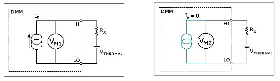
This measurement involves two cycles. One is measured with the current source on, as shown in Figure 13. The second is with the current source off, as shown in Figure 14. The net result is the difference between the two measurements. Because the offset voltage is present in both cycles, it is subtracted out and does not enter into the resistance calculation, as shown below.
VOCO = VM1 - VM2 = (ISRX + VTHERMAL) - VTHERMAL = ISRX
therefore:
RX = VOCO/IS
Conclusion
NI developed the high-performance, single-slot 3U PXI-4081 FlexDMM based on its FlexADC technology. Many of the traditionally error-prone analog functions of conventional DMMs have been replaced by using a commercially available high-speed digitizer, DSP technology, and the power of the host computer. Self-calibration provides optimum accuracy over the full 0 to 55 ºC operating temperature range with a two-year calibration cycle. Combined with highly stable built-in reference elements, the result is the world’s fastest, most accurate PXI DMM, with uncompromised features and performance rivaling and exceeding that of most traditional DMMs.