An Introduction to High-Throughput DSP in LabVIEW FPGA
Overview
Modern FPGAs offer considerable resources for implementing real-time digital signal processing (DSP) algorithms, and the NI LabVIEW FPGA module offers significant advantages for FPGA-based DSP design over other design flows. This paper will describe an efficient design process for developing DSP algorithms on NI FPGA hardware in LabVIEW FPGA. The design of a simple FIR filter will be used as a case study throughout this process.
Contents
DSP Design Process
While LabVIEW programming for desktop PCs does not necessarily dictate a structured development process, programming for FPGA targets without a proper design flow can lead to significant inefficiency due to the long compilation times incurred between algorithm design and test. The method outlined below focuses on reducing the number of compiles through proper simulation techniques. Basic steps include developing a behavioral model of the DSP algorithm, creating structural IP for FPGA-based implementation, simulation of the structural IP on a desktop PC, compiling the IP for an FPGA, and finally testing of the design on FPGA hardware. The last stage of hardware-based testing can be further divided into hardware co-simulation and testing with real-world I/O.
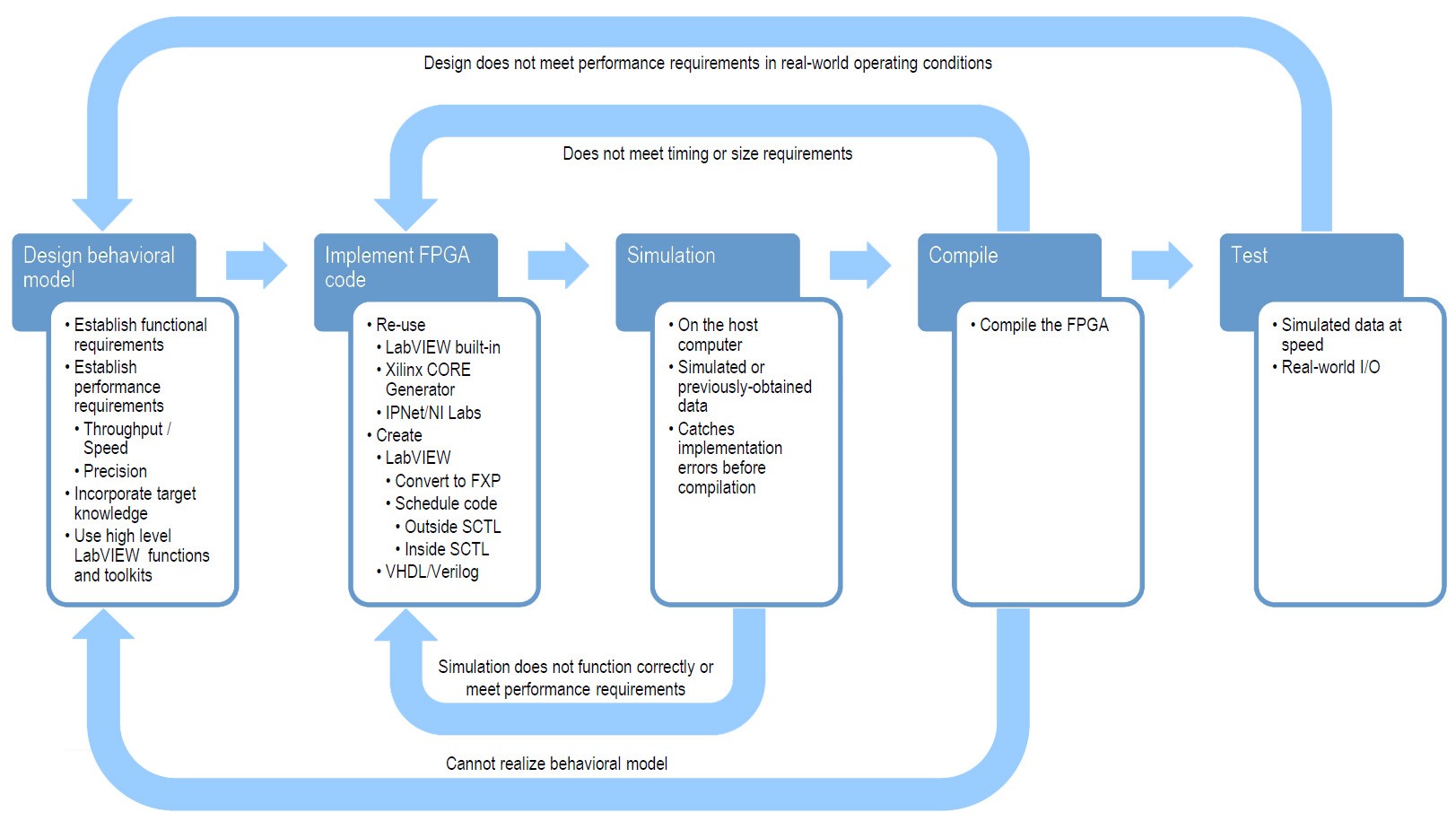
Figure 1. A LabVIEW FPGA DSP design process
There are also feedback paths throughout the process if certain criteria are not met. The first path feeds back from simulation to structural IP creation, when any errors in the design are observed in simulation. Next, if a compilation fails by not meeting timing or space requirements, refinement must be made in the structural IP. If all possible optimizations are exhausted and the design cannot fit on a given FPGA target, then either another FPGA must be chosen, or the overall system architecture must be re-evaluated, adding FPGAs to the system, or moving components of the processing to other targets such as microprocessors or GPUs. Finally, for successfully compiled designs, errors may be found when real-world I/O is incorporated, which requires the initial performance requirements to be re-evaluated.
Behavioral Model
The purpose of the behavioral model is to establish performance criteria and validate the correctness of a design without regard to how it might be implemented in hardware. This validation is performed on the desktop PC, and it is appropriate to use existing, known-good algorithms as references. Examples of performance criteria are sample rate, bandwidth, quantization noise, dynamic range, distortion, spurs, phase noise, frequency resolution, filter pass band ripple, stop band rejection, transition band slope, etc. Design parameters might include attributes such as bit widths (for sampled data), filter lengths and coefficients, transform lengths and parameters, waveform generator and detector attributes, mathematical formulas, etc. With these details in mind, it is also important to perform a sanity check on the design to ensure that it is likely to fit and meet timing on a given FPGA. For instance, the sample rate may dictate FPGA clock rates, while noise, dynamic range, bit widths, and transform lengths can impact resource utilization including optimized DSP resources and on-FPGA block RAM. Confirming that a given design is indeed realizable in hardware can save time and frustration in subsequent stages of the design process. To do this, one might look to the specified amount of limited hardware resources (DSP slices and block RAM), prior experience with design complexity and size estimates, and resource utilization and performance of comparable designs available from public IP sources and NI Labs).
One limitation of FPGAs is that they do not typically include dedicated resources for operating on floating point numbers, which are extremely common in microprocessor-based DSP algorithms. While FPGAs can implement floating point numerical operations in general-purpose logic slices, this consumes significant resources and limits the amount and complexity of the realizable signal processing. Instead, it is common to use fixed-point representations which allow fractional data, but do not require the additional resources of a floating point representation. The main limitation of fixed point data is a limited dynamic range, though this can be overcome by adding bits at appropriate stages in the signal processing flow. This paper will not cover fixed point operations in detail, but additional information can be found on ni.com, as well as on Wikipedia.com. What is particularly relevant to this stage of the FPGA DSP design process is that fixed point representations be validated in the behavior model. This typically means coercing all data to a fixed-point resolution and dynamic range, then sending it through existing floating point algorithms written for a microprocessor. While not explicitly accurate (bit-true), this serves as a very good approximation of fixed-point bit width requirements, and bit-true simulations will be run in subsequent structural simulations for final confirmation.
For this paper we will evaluate the design of a finite impulse response (FIR) filter, with the following performance criteria:
- Data source: 250 MS/s, 16-bit ADC
- 10 MHz bandwidth
- < 1 dB ripple
- > 30 MHz stop band
- > 65 dB attenuation
The main variables of this design will be the FIR filter length and filter coefficients. The NI LabVIEW Digital Filter Design Toolkit is an excellent tool for filter design, and the Classical Filter Design Express VI makes the design of a filter with these properties a very simple process:
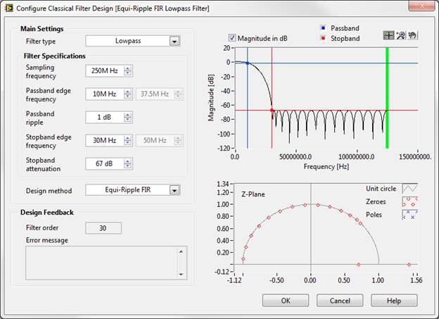
To achieve better than the desired performance criteria, we see that it will require a 30th order filter. For an FIR filter, this means that for each new sample, it and the 30 prior contiguous samples must be scaled by a coefficient, then summed to produce a single sample output. Looking at the DSP resources for the NI PXIe-7965R FPGA Module, we see that there are 640 DSP slices available, so this filter, which will only consume 31 DSP slices, should fit without issue.
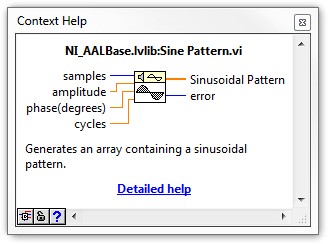
Also necessary for a behavioral simulation are a stimulus signal source, as well as an existing FIR filter implementation. A simple variable sinusoidal stimulus should prove sufficient for basic filter testing. LabVIEW has numerous methods of generating sinusoids, and the Sine Pattern VI is one such function.
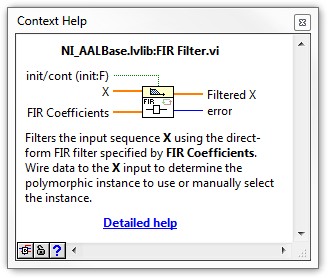
There is also a built-in FIR Filter VI which can be used to filter both the floating point representation of the stimulus signal and coefficients, as well as the coerced fixed-point representation.
In order to coerce the floating point representation to a fixed-point resolution and dynamic range, simply convert to a specific fixed point representation (grey), then back to floating point (orange).
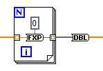
Because the To Fixed-Point VI does not operate on array data types, we must place it inside an auto-indexed for loop. To set the fixed point representation, simply right-click on the constant wired into the To Fixed-Point VI, select Properties, then the Data Type tab to set signed or unsigned encoding, as well as the number of total and integer bits.
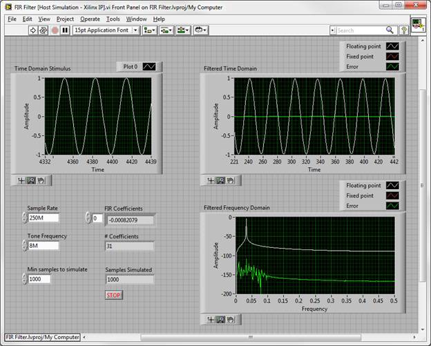
By comparing a behavioral simulation using all floating point numbers to one with the stimulus samples and filter coefficients coerced to fixed point, we can observe the performance impact of a specific fixed point representation. Below is a simulation with a relatively low bit width fixed point representation, using 8 bits for the data, and 10 bits for the coefficients.
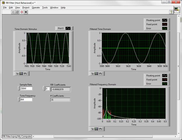
The floating point output is plotted in white, the fixed point in red, and the difference between the two, or the error signal, in green. While this limited resolution yields surprisingly good results, spurious artifacts approach the 65 dB stop band requirement. Knowing that the DSP slices of the Xilinx Virtex-5 FPGAs include a 25 bit by 18 bit multiplier, it is common practice to represent coefficients with 18 bits, and the data with 25, accommodating any bit growth prior to the filter. Anything less would essentially waste resources. For this design, since the filter will be immediately after a 16-bit ADC, here are the results from a simulation with 16-bit data and 18-bit coefficients:
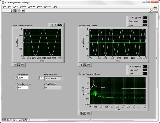
Note the change in scale of the frequency domain plot, and the significantly lower error. This fixed point representation is sufficient for the above performance criteria. Additional testing of the behavioral model should be performed at this point to confirm pass band, stop band, and transition band performance, as well as any other care-abouts. Furthermore, it is a good idea to capture a test waveform from the ADC in question and send it through the behavioral model. This will incorporate real-world performance data early in the design cycle, and help ensure that nothing was missed in the high-level algorithm design.
Structural Model
Once the design parameters of the behavioral model of an algorithm have been confirmed, they must be translated into a structural implementation. In addition to the fixed point data representation simulated in the behavioral model, there are numerous other considerations which must be taken into account when porting an algorithm from a microprocessor to an FPGA. While microprocessor hardware is architected to be very versatile with 10s of pipeline stages, capable of executing functions defined by 1000s of instructions, FPGAs implement specialized hardware structures for each phase of an algorithm, often implemented as a pipeline 100s or 1000s of elements deep. In other words, while the same small number of pipelined stages on a microprocessor can run programs of arbitrary length, due to limited space on an FPGA, there are a limited number of distinct functions or operations possible, and hence an upper bound on the “length” or complexity of an algorithm. Additionally, microprocessor algorithms, with their specific memory architecture, tend to operate on large vectors of data at a time, often only performing a few mathematical operations at once. In contrast, FPGA algorithms tend to operate point-by-point, running a single data point through the entire hardware pipeline without any temporary data storage. While it is possible to implement algorithms which do require memory in-line, it is a scare resource on the FPGA, so the depth of such operations is limited. Moving data to a much larger off-FPGA DRAM is another option, but often places constraints on throughput and latency. More often, such off-FPGA DRAM is used for buffering data before or after processing, allowing operation on larger contiguous data sets.
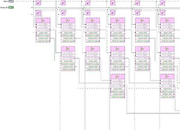
Apart from overall algorithm architecture, the next most important considerations for an FPGA structural implementation are the desired processing throughput, and the necessary clock rate. Clock rate is specified by the clock used to execute the logic in a Single-Cycle Timed Loop (SCTL).
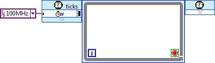
All logic for a given algorithm generally exists within a single SCTL, and pipeline stages are delineated with shift registers, feedback nodes, or feed forward nodes.
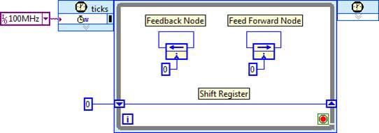
In the above image, these structures are initialized to zero, and do not perform any useful operations (effectively a NOP) between loop iterations (clock ticks). In an actual algorithm, operations would be inserted between these structures, and multiple nodes would be connected together to implement a processing pipeline. In the most straightforward implementation of an algorithm, the clock rate is set to the desired throughput, such that one data point is processed for each clock tick.
With current Virtex-5 FPGAs and LabVIEW FPGA 2011, designs up to 250 MHz are attainable, though as the clock rate exceeds 200 MHz, more and more attention must be paid to the critical path – the longest propagation delay between pipeline stages of the algorithm. When a clock rate cannot be achieved which meets or exceeds the desired throughput, the algorithm must be parallelized, and multiple data points processed each loop iteration:
Of course, this may have significant implications on the algorithm, requiring re-factoring of any operations with point-to-point dependencies. Similarly, if there are operations in an algorithm which are re-used multiple times, and those operations can execute at clock rates significantly greater than the desired throughput, resources can be re-used, decreasing the overall resource requirements.
Additional logic must be used for arbitration, however, the complexity depending on how that operation is used in the algorithm.
Another consideration, as mentioned previously, is the bit width. Microprocessors are typically specified as 8, 16, 32, or 64-bit, which refers to the width of their general-purpose data path. FPGAs have an advantage in that they can support arbitrary data widths – whatever is necessary for the desired operation. This enables more efficient resource utilization, and for designs which fill the FPGA, no more resources should be used than absolutely necessary.
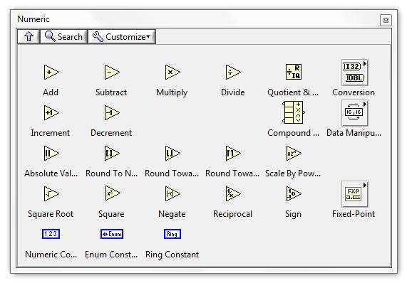
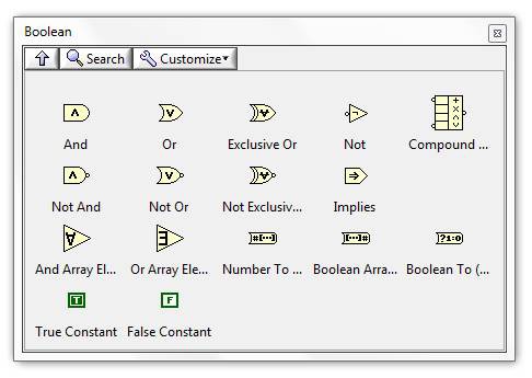
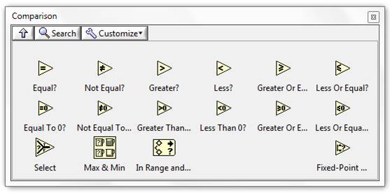
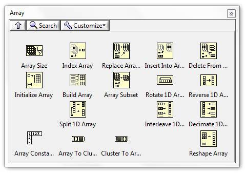
When it comes to actually implementing an algorithm, the LabVIEW FPGA palettes for Numeric, Boolean, Comparison, and Array primitives offer the majority of operations necessary. Most of these primitives can be used inside a single-cycle timed loop, though the LabVIEW Help should be consulted for confirmation.
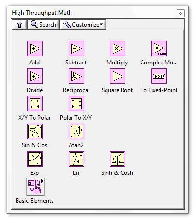
In addition to these primitives, for very high clock rate designs, the High-Throughput Math palette offers fully-pipelined numerical operations.
In addition, these operations support the 4-wire handshaking protocol. The 4-wire handshaking protocol is a superset of the 2-wire handshaking protocol, which couples input data valid and output data valid Boolean signals with input and output data. This allows the operation to accommodate data throughput less than the clock rate, only processing on loop iterations / clock cycles in which the data is valid. Full 4-wire handshaking extends this protocol further, allowing downstream IP to signal when it is ready for new data, and also serves as a means to signal when it is acceptable for upstream IP to produce new data. The full 4-wire protocol is useful for interfacing operations with different throughputs.
Finally, to achieve the absolute highest performance, you can use the DSP48E node to directly control the dedicated DSP hardware on the FPGA.
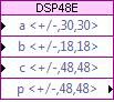
While this offers the highest performance, it introduces significant design complexity, and also ties the design to a specific FPGA target, limiting future algorithm portability.
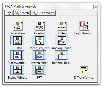
Of course, if IP exists for the desired algorithm, then there is no need to implement it from scratch. There are a number of sources for this IP. First and foremost, a number of common functions exist on the FPGA Math and Analysis palette, with various levels of performance.
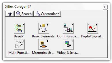
For IP written in LabVIEW and ni.com/labs have algorithms developed by NI, as well as those submitted by the LabVIEW FPGA community of developers. Additionally, the aforementioned Digital Filter Design Toolkit can also synthesize FPGA filters. For IP completely optimized for Xilinx FPGAs, however, there is no better source than the Xilinx IP palette, which provides simple and direct integration of Xilinx CORE Generator IP.
Specific to DSP, there are a number of operations which are extremely useful, in particular the FIR filter and FFT IP.
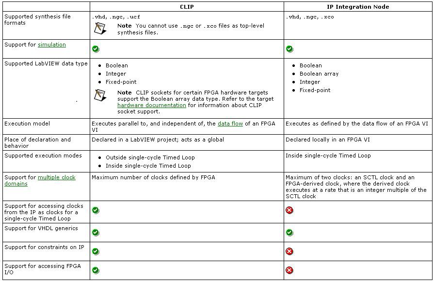
Finally, for importing existing HDL, there are two options: the IP Integration Node, and the Component-Level IP (CLIP) Node. The IP Integration Node is designed for importing IP which has a synchronous interface to the LabVIEW diagram and operates in the same clock domain as the SCTL in which it resides, in a dataflow manner. The CLIP Node is designed as an asynchronous interface to IP, and can accommodate multiple internal clock domains, as well as interface to the LabVIEW diagram in multiple clock domains.
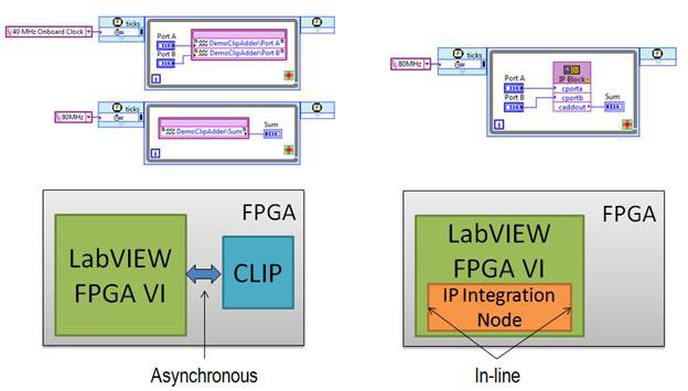
The IP Integration Node has the added benefit of bit-true, cycle-accurate simulation on the development computer, while the CLIP Node requires a third-party simulator for proper simulation. A further comparison can be found in the table below.
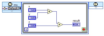
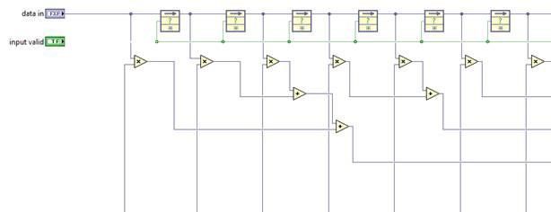
Returning to the simple FIR filter case study, there are a number of ways to implement an FIR filter with the methods described above. It can be implemented with basic LabVIEW primitives.
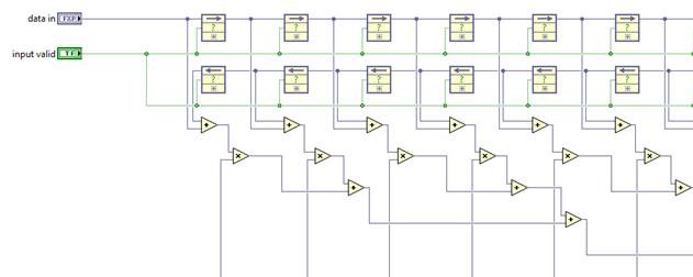
Though without any explicit pipeline stages between the first multiply and the consecutive additions, the critical path of this design will be very long, and the achievable clock rates and throughput very low. A more efficient implementation would be a re-structuring of this adder chain with a more hierarchical structure.
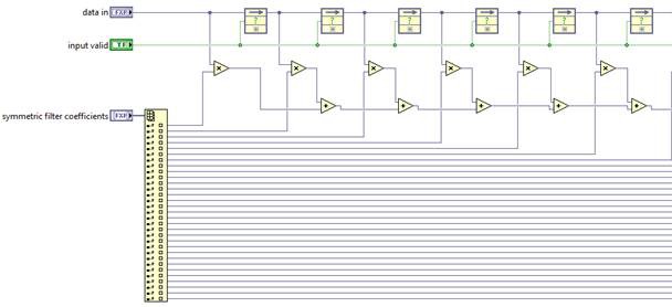
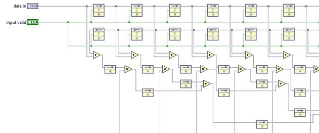
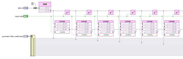
Or you can take such algorithmic optimizations even further and exploit symmetry in the FIR coefficients, summing input samples before scaling by common coefficients. This reduces the number of multipliers necessary.
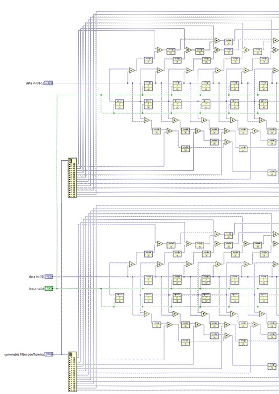
While more efficient, these designs may not have a significant input in the critical path, as there is still a path containing a multiplication and several additions. Pipelining can break this up further.
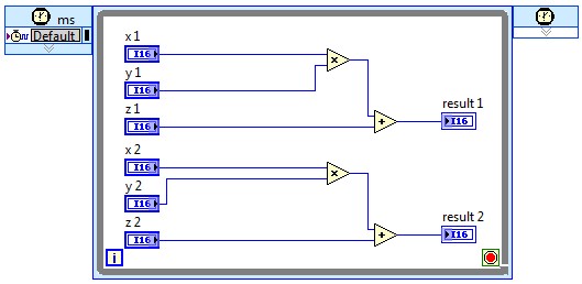
And we should expect a much higher achievable clock rate. If the resulting throughput is not high enough, the FIR algorithm can be parallelized.
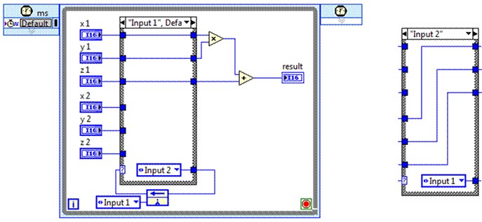
This effectively sets the throughput at double the clock rate, at the expense of additional resource utilization. If algorithm parallelization is not an option, the high-throughput math palette might provide higher performance.
Note that this uses only 2 of the 4 handshaking wires, effectively implementing 2-wire handshaking, similar to the above implementations. Finally, for the absolute highest level of performance, the DSP48E node provides very efficient use of the multiply and accumulate structure of the Xilinx DSP slice for very high clock rates.
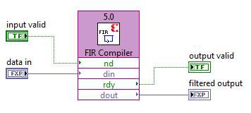
Finally, since the FIR filter is a very common function and Xilinx has CORE Generator IP for it, and this is available on the LabVIEW FPGA Xilinx IP palette.
The coefficients designed with the Digital Filter Design Toolkit can be easily imported into the Xilinx FIR Compiler by using a helper example VI which outputs a *.coe file. This helper VI can be found here:
C:\Program Files\National Instruments\LabVIEW 201*\examples\Digital Filter Design\Fixed-Point Filters\Multirate\Export Multirate FIR Coef to Xilinx COE File.vi
Achievable throughput for the designs above will be evaluated in the Compilation section below, but before compiling, the design should be simulated to confirm similar performance to the behavioral model.
Simulation
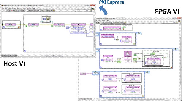
There are several methods for desktop PC simulation of FPGA IP, but for high-throughput DSP algorithms in the single-cycle timed loop, one specific method tends to be the most efficient. This technique runs the FPGA VI on the host computer in a “dataflow-accurate” manner. Dataflow-accurate basically means that all dataflow paradigms are obeyed, and the simulation is cycle-accurate within the context of a single SCTL. Furthermore, the simulation is also bit-true, meaning that the results are numerically identical to those obtained when running on FPGA hardware after a successful compilation. In addition to the FPGA VI running on the host, there is also a separate host VI which serves as the test bench, sending stimulus waveforms to the FPGA VI, and capturing and displaying the results. This VI can often leverage significant components of the existing host-based behavioral simulation described above.
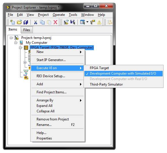
To execute the FPGA VI on the host in simulation mode, simply right click on the FPGA target in the LabVIEW project, then select “Execute VI on -> Development Computer with Simulated I/O”.
This will ensure that when the host test bench opens a reference through the NI-RIO driver to the FPGA VI under the simulated FPGA target context, it will simply run it on the host as opposed to initiating a lengthy compilation. In order to send and receive stimulus and response data from the host test bench, you also use the NI-RIO driver Invoke Methods for DMA FIFOs. These correspond to FPGA FIFOs on the FPGA VI.
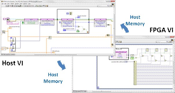
In the above host test bench and FPGA VI, the “Host to FPGA FIFO” is used to send data to the FPGA VI for processing, and the “FPGA to Host FIFO” (not pictured on the FPGA VI) is used for capturing and displaying simulation results. This method uses host-based memory buffers to transfer these test waveforms between the host test bench and the FPGA VI being simulated. While the FPGA VI has the usual limited set of functions, the host test bench has access to the full array of LabVIEW functions for waveform synthesis, analysis, and display. This enforcement of target-specific functions prevents the FPGA VI from being muddled with operations which cannot be synthesized on hardware and could potentially mask design errors, while providing the host test bench with the flexibility to bring in a vast library of debugging utilities.
Again, significant components of the host behavioral model can be re-used for the test bench, especially the floating point model as a basis for comparison. The output of the fixed point coercion model is typically replaced with the necessary NI-RIO calls to obtain that same data from the FPGA VI simulation. In the case of the FIR filter, when using either the Xilinx IP or the FIR structures implemented with LabVIEW primitives, the FPGA VI simulation matches the behavioral simulation very well, with minimal error.
Catching structural errors at this stage of the design can be corrected and re-simulated with a very tight turn-around time – as low as minutes. This enables multiple iterations to quickly validate the structural IP, without lengthy compilation cycles in the design loop.
Compilation
After the structural IP simulation matches the behavioral model, LabVIEW features a 1-click compilation process to create a bitfile for the given design. Depending on the complexity of the design, the compilation could take as little as 10 minutes, to upwards of 5 hours. The compilation window will provide size and timing estimations before and after synthesis, and after map and place and route, increasing in accuracy with each estimate. It will also provide a final summary which indicates whether or not the compile succeeded, and if it did not, whether the failure was due to size or timing.
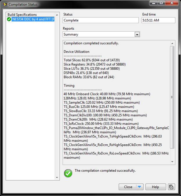
For timing failures, there is an option to highlight the critical path, which provides a graphical illustration on the LabVIEW diagram of the longest propagation delay(s) of the design. These critical paths should be broken up with pipelining or algorithm parallelization. Another timing-related optimization for Xilinx IP or the IP Integration Node is to disconnect the IP Enable and Asynchronous Reset signals in the configuration dialogs, after structural simulation is complete and immediately before compilation. This reduces the fanout of some LabVIEW-provided enable and reset signals, decreasing critical path length. If this must be done to meet timing, the reset behavior of the IP must be well understood, and it should only exist in free-running SCTLs (no data dependencies, and no stop condition on the loop). For designs which do not fit on the FPGA, techniques such as resource arbitration should be investigated, else operations should be moved off the FPGA and on to other targets (host microprocessor or additional FPGAs). Finally, if none of these techniques produce a design which meets the original performance criteria, then these criteria must be re-evaluated, and the behavioral model re-visited.
For newly-developed or configured IP, it is often worthwhile to compile the FPGA VI used for simulation of the structural model. This enables a technique called hardware co-simulation, which can be valuable for running very long simulations to more exhaustively validate the IP.
Hardware Co-Simulation
Hardware co-simulation can be thought of as accelerating the structural IP simulation by running it on actual FPGA hardware. Because of the versatility of the NI-RIO driver, this simply means compiling the FPGA simulation VI for a specific target, and configuring that target in the project to run on real hardware, as opposed to simulation on the host. In addition to providing true cycle-accurate simulation (though this should not be necessary if the algorithm obeys dataflow programming), the simulation occurs at a much higher rate, allowing you to simulate a greater number of points in the same amount of time, with the same debugging information developed in the host test bench. Once the IP being developed becomes relatively static (little to no changes in the source), then the slower host simulation can limit validation efficiency. By compiling this FPGA VI, you can accelerate these simulations with hardware, provided this signal processing implements at least 2-wire handshaking, if not the full 4- wire handshaking protocol. This is because the host testbench will be running much slower than the FPGA VI, and it will not be able to source or sink data as fast as the loop rates of the FPGA. In other words, the FPGA will be running at speed (100s of MHz), but only processing simulation data as fast as the host can supply it. Of course, instead of using host memory to transfer data between the host test bench and the FPGA VI, hardware co-simulation uses a real hardware bus to transfer data to and from the FPGA, such as PXI express.
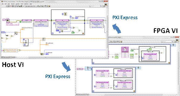
Again, in this scenario neither the host test bench VI nor the FPGA VI must change. The FPGA VI need only be compiled. This is also a good opportunity to simulate longer real-world waveforms previously acquired, introducing the artifacts of real I/O while still simulating, enabling quick re-production and debug of any anomalous results.
For the FIR filter described above, hardware co-simulation results match the host simulations exactly. Iterating on the different implementations, the following maximum clock frequencies were obtained, with the associated resource utilizations.
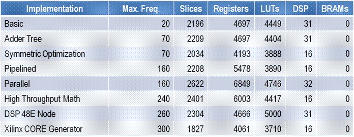
From these results, we see that only the implementations using the Xilinx CORE Generator, the DSP48E node, or the parallel architecture can meet the desired throughput. Of these, comparing the resource utilization, the Xilinx CORE Generator is the most efficient implementation.
Real I/O
Once the algorithm has been completely simulated, with or without hardware, and the effects of incorporating real I/O are well-known, through simulation with real-world waveforms, this I/O can be connected to the algorithm and a new FPGA bitfile generated. If the real I/O is via peer-to-peer data streaming, then the FIFOs used in the FPGA simulation VI need only be replaced with peer-to-peer FIFOs of the appropriate direction. If the I/O is connected directly to the FPGA through, say, a FlexRIO adapter module, then the simulation FIFOs should be replaced with I/O nodes, and the SCTL clock configured to be the appropriate clock for those I/O nodes (usually an ADC or DAC clock, provided on IOModuleClock0 or 1). An alternative method is to leave the IP in its original clock domain, then place the I/O in other SCTLs with the associated clocks, using local FIFOs to pass around data. This may be done because the I/O clock may not be free-running, and unstable clocks could put the algorithm into an unknown state, or because host-to-FPGA and FPGA-to-Host FIFOs may be difficult to compile at the highest clock rates. This technique can even be taken a step further, conditionally sending either real data (to and from the I/O) or simulation data (to and from the host, for hardware co-simulation) through the algorithm. At any rate, for an algorithm connected to an ADC, in this scenario other test and measurement equipment such as an arbitrary waveform generator or function generator will provide the stimulus, while the results will be sent through the host through a bus such as PXI Express.
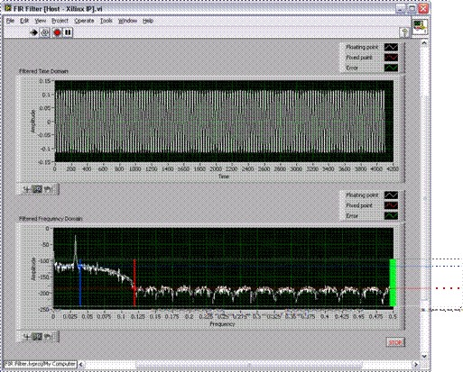
Assuming the I/O does not introduce any compilation issues, the final design should be ready to run, and the results should match the original behavioral model. For the FIR filter, we see that the actual frequency domain response identically matches the filter response created by the Digital Filter Design Toolkit.
Conclusions
This paper is designed to be a high-level overview of implementing high-throughput DSP algorithms in LabVIEW FPGA. It focuses on proper simulation techniques to maximize developer efficiency. While these techniques do require additional up-front investment, very few designs succeed on the first compile, and the additional time spent on simulation quickly pays for itself in time not spent waiting on multiple compilations to complete. This paper also does not go into significant depth on many of the topics covered, but rather provides a high-level overview. More information on these techniques can be found through in-line links, in the LabVIEW FPGA help, or by searching ni.com