Testing and Debugging LabVIEW FPGA Code
Overview
The LabVIEW FPGA Module includes several simulation options. It is important to understand when and how to use each option in the design verification process. This document helps you make decisions about using the different LabVIEW FPGA simulation options for testing a design.
Contents
- Modular Testing Levels
- Understanding FPGA Execution Modes
- Choosing an FPGA Execution Mode
- Execution in the Windows Context
- Execution in FPGA Simulation Mode
- Execution in a Third-Party Simulator
- Execution on the FPGA Target
Modular Testing Levels
Verification of large and complex applications can be simplified by breaking the code down into modular sections. By testing smaller, simpler modules first, you can identify functional problems that are more challenging to diagnose in a full system test. Testing is divided into three levels: unit, component, and system.
Unit
The unit is the most fundamental level of IP as it serves a specific function and cannot be further decomposed for testing. Typically a unit is a specific algorithm or processing function composed of various language primitives.
A section of code is a unit if the code meets the following requirements:
- The code can be encapsulated as a subVI that you may want to reuse in another part of the design.
- The code does not include I/O, data communication, or any target-specific resources.
- The code does not have multiple loops running in parallel or at different rates.
- The function of the code can be verified by providing a set of known inputs to test for expected outputs.
- The state of the code does not rely on the explicit passing or control of time.
Component
Components are more complex pieces of logic that include elements that can affect the timing or state of the entire system. An FPGA application can usually be broken down into multiple components whose functionality can be verified individually before they are integrated into a larger component.
A section of code is a component if the code meets the following requirements:
- The code has a clear and narrow task or objective to accomplish.
- The code is a single process and its execution stands alone or the code is a collection of processes dependent on one other.
System
The system is the top-most component, which is represented by the top-level FPGA VI plus any additional IP imported into the design through Component-Level IP (CLIP). Only the interface of the top-level FPGA system is exposed to the host application. As a result, verification tests typically require connection to the host interface API and real I/O signals. A system usually contains multiple components working together to accomplish a set of tasks.
Understanding FPGA Execution Modes
The LabVIEW FPGA Module includes several execution modes. Each execution mode offers different functionality for testing and debugging an FPGA VI. You can change the execution mode by right-clicking the FPGA target in the LabVIEW project and selecting Select Execution Mode from the shortcut menu.
Note: The FPGA Desktop Execution Node is not available in a real-time environment.
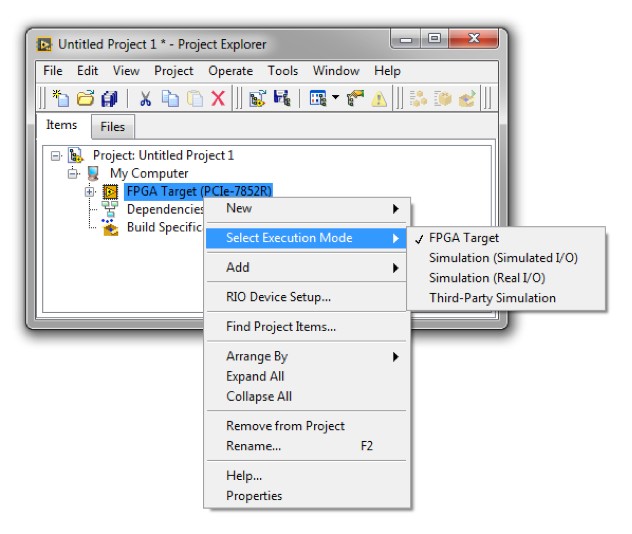
Figure 1. Selecting Execution Mode within the LabVIEW FPGA project.
FPGA Target
Executing on the FPGA hardware is typically reserved for the final stages of testing a LabVIEW FPGA design. This execution mode is the most representative of how a system will behave in deployment, however debugging options are limited mode.
Simulation (Simulated I/O)
Most LabVIEW FPGA users will execute the majority of testing in this mode. Simulation mode utilizes an advanced simulation engine to execute a VI on the desktop, but with timing characteristics similar to the FPGA hardware. Simulation mode with simulated I/O offers several advanced mechanisms for validating code with simulated values for I/O. The simulated values can be arbitrary or defined.
Simulation (Real I/O)
In this mode, real data is acquired from the inputs of the FPGA target, passed to the host computer, and consumed in the simulation environment. Changing FPGA output values in simulation results in the physical changes to the FPGA hardware output. This execution mode is reserved for R Series targets only.
Third-Party Simulation
This execution mode relies on advanced third-party software and VHDL test benches to provide a full cycle-accurate simulation of FPGA code. Third-party simulation mode also allows for verification of HDL IP integrated through the CLIP or IP Integration Node.
Choosing an FPGA Execution Mode
With a basic understanding of modular testing levels and FPGA execution modes, you can determine which execution mode is appropriate for testing each part of a LabVIEW FPGA design. The following table summarizes the ideal usage of each execution mode:
| Execution Mode | Windows PC1 | FPGA Simulation Mode | Third Party Simulation | FPGA Target |
|---|---|---|---|---|
| Verify Functional Performance | ✓ | ✓ | ✓ | ✓ |
| Verify Timing | ✓2 | ✓ | ✓ | |
| Verify Third Party HDL IP | ✓3 | ✓ | ✓ | |
| Good for Unit Testing | ✓ | |||
| Good for Component Testing | ✓ | ✓ | ✓ | |
| Good for System Testing | ✓ |
1 Windows PC is not found in the Select Execution Mode shortcut menu. Refer to the Execution in the Windows Context section for details.
2 FPGA simulation mode uses the concept of simulated FPGA time. Refer to the Execution in FPGA Simulation Mode section for details.
3 Only simulation of IP integrated through the IP Integration Node is supported in FPGA Simulation Mode. For simulating CLIP, NI recommends using third party simulation.
Execution in the Windows Context
Execution of a VI in the Windows context is primarily used for unit testing and logic validation. Because a unit does not contain any FPGA-specific I/O or resources, you can execute the VI in the Windows context. To execute an FPGA VI in the Windows context, click and drag the VI from the FPGA target to My Computer in the LabVIEW project.
Once you move the VI, you can create a test bench VI to exercise the functionality of the unit. Because you execute the VIs in the Windows context, the test bench can contain functions that do not exist in the FPGA context and you can create UIs to visualize test results.
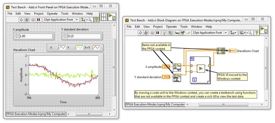
Figure 2. Unit testing using LabVIEW on a Windows environment.
When you execute an FPGA VI in the Windows context, you can only verify the functionality of the VI. In the Windows context, none of the FPGA timing characteristics of the VI is preserved. To verify timing, you must integrate the unit into a component and test the unit in one of the other execution modes.
Execution in FPGA Simulation Mode
FPGA simulation mode provides the ability to simulate FPGA I/O and resources and allows for better understanding execution timing. These factors make FPGA simulation mode ideal for testing code components.
NI recommends that you create a test bench VI that runs on the host, such as My Computer or RT Target, which interfaces with the FPGA VI running in simulation mode. By running a test bench VI on the host, you can access hundreds of functions for creating test inputs and analyzing test results. You can also use these functions to create or import a reference implementation of your component. The following figure shows a high-level diagram of a test bench that you can implement graphically in LabVIEW:
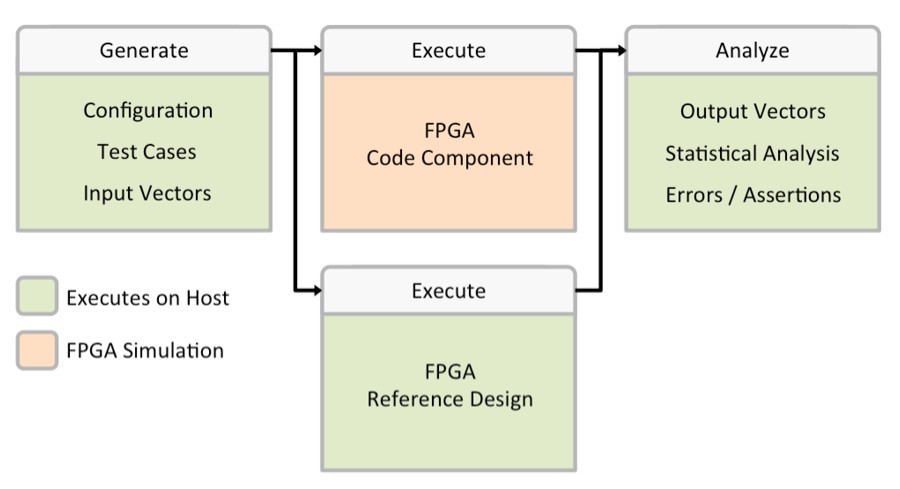
Figure 3. LabVIEW FPGA Simulation Mode using a test bench environment.
In LabVIEW 2013, the FPGA Desktop Execution Node (DEN) was introduced to simplify creating host test benches and improve simulation timing of FPGA code. The DEN uses simulated time to reflect timing in hardware. You can use the DEN to provide customized stimuli to controls and inputs, force FPGA time to advance a set number of ticks, and then read the values of indicators and outputs. You can easily iterate on this procedure to validate a component using a range of test vectors and cases.
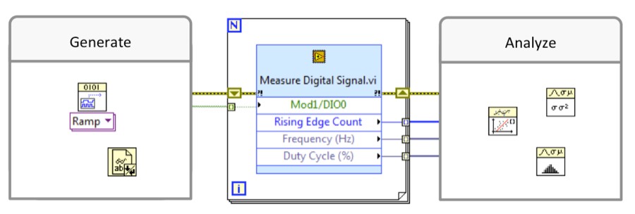
Figure 4. Using Desktop Execution Node to simplify test bench environment including improved timing capabilities.
Refer to the Using the LabVIEW FPGA Desktop Execution Node tutorial for more information about the FPGA Desktop Execution Node.
Execution in a Third-Party Simulator
To meet advanced simulation requirements, you can interface LabVIEW FPGA with third-party simulation software. Third-party simulation provides true, cycle-accurate simulation of FPGA designs for in-depth timing analysis. Third-party simulation also provides the most useful simulation of designs containing IP integrated through the CLIP or IP Integration Node. The following figure shows a high-level diagram of third-party FPGA simulation:
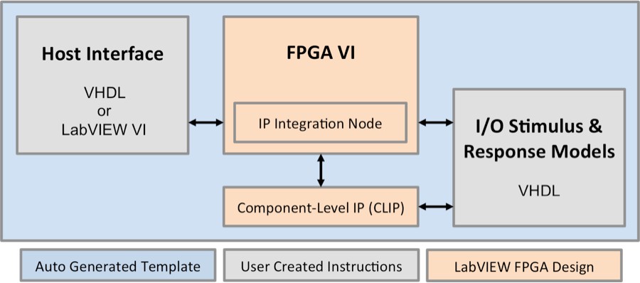
Figure 5. Third party code integration using CLIP or IP Integration Node.
Xilinx ISim (ISE) and Xilinx XSim (Vivado) are included with the LabVIEW FPGA Compilation Tools. Xilinx ISim and Xilinx XSim require knowledge of VHDL to write effective test benches. Refer to the Cycle-Accurate Simulation With Xilinx ISim document for more information about using Xilinx ISim.
Using LabVIEW to create a host interface test bench for third-party simulation increases productivity and eliminates the need for VHDL expertise.
Note: Support for Mentor Graphics Questa Simulator has been dropped as of the release of the LabVIEW 2018 FPGA Module.
Execution on the FPGA Target
As with any system, full verification requires testing not only in a simulation environment, but also on hardware. Executing on the physical hardware provides the most accurate representation of how the design will behave in a deployed environment because it is subject to actual I/O, jitter, and other things that can affect system functionality or timing.
Because traditional LabVIEW debugging tools are not available on a physical FPGA target, you must compile mechanisms into your design to help you validate functionality and timing. The following mechanisms are helpful for verifying FPGA physical execution:
- Use indicators and FIFOs to pass data from key areas up to the host.
- Use controls, loops, and sequence structures to create triggers to “pause” FPGA execution.
- Use sequence structures and tick counters to benchmark timing in critical sections of code.
- Use Xilinx ChipScope to probe, trigger, and view internal FPGA signals.