PXIe-5785 Specifications
- Updated2025-05-06
- 13 minute(s) read
PXIe-5785 Specifications
Definitions
Warranted specifications describe the performance of a model under stated operating conditions and are covered by the model warranty.
Characteristics describe values that are relevant to the use of the model under stated operating conditions but are not covered by the model warranty.
- Typical specifications describe the performance met by a majority of models.
- Nominal specifications describe an attribute that is based on design, conformance testing, or supplemental testing.
- Measured specifications describe the measured performance of a representative model.
Specifications are Typical unless otherwise noted.
PXIe-5785 Pinout
Use the pinout to connect to terminals on the PXIe-5785.

| Signal | Type | Direction |
|---|---|---|
| MGT Tx± <0..3> | Xilinx UltraScale GTH | Output |
| MGT Rx± <0..3> | Xilinx UltraScale GTH | Input |
| DIO <0..7> | Single-ended | Bidirectional |
| 5.0 V | DC | Output |
| GND | Ground | — |
Digital I/O
Connector | Molex™ Nano-Pitch I/O™ |
5.0 V Power | ±5%, 50 mA maximum, nominal |
| Signal | Type | Direction |
|---|---|---|
| MGT Tx± <0..3>1 Multi-gigabit transceiver (MGT) signals are available on devices with KU040 and KU060 FPGAs only.[1] | Xilinx UltraScale GTH | Output |
| MGT Rx± <0..3>[1] | Xilinx UltraScale GTH | Input |
| DIO <0..7> | Single-ended | Bidirectional |
| 5.0 V | DC | Output |
| GND | Ground | — |
Digital I/O Single-Ended Channels
Number of channels | 8 |
Signal type | Single-ended |
Voltage families | 3.3 V, 2.5 V, 1.8 V, 1.5 V, 1.2 V |
Input impedance | 100 kΩ, nominal |
Output impedance | 50 Ω, nominal |
Direction control | Per channel |
Minimum required direction change latency | 200 ns |
Maximum output toggle rate | 60 MHz with 100 μA load, nominal |
| Voltage Family (V) | VIL (V) | VIH (V) | VOL (100 µA Load) (V) | VOH (100 µA Load) (V) | Maximum DC Drive Strength (mA) |
|---|---|---|---|---|---|
| 3.3 | 0.8 | 2.0 | 0.2 | 3.0 | 24 |
| 2.5 | 0.7 | 1.6 | 0.2 | 2.2 | 18 |
| 1.8 | 0.62 | 1.29 | 0.2 | 1.5 | 16 |
| 1.5 | 0.51 | 1.07 | 0.2 | 1.2 | 12 |
| 1.2 | 0.42 | 0.87 | 0.2 | 0.9 | 6 |
Digital I/O High-Speed Serial MGT[3]3 For detailed FPGA and High-Speed Serial Link specifications, refer to Xilinx documentation.
Data rate | 500 Mbps to 16.375 Gbps, nominal |
Number of Tx channels | 4 |
Number of Rx channels | 4 |
I/O AC coupling capacitor | 100 nF |
Reconfigurable FPGA
PXIe-5785 modules are available with multiple FPGA options. The following table lists the FPGA specifications for the PXIe-5785 FPGA options.
| KU035 | KU040 | KU060 | |
|---|---|---|---|
| LUTs | 203,128 | 242,200 | 331,680 |
| DSP48 slices (25 × 18 multiplier) | 1,700 | 1,920 | 2,760 |
| Embedded Block RAM | 19.0 Mb | 21.1 Mb | 38.0 Mb |
| Data Clock Domain | 200 MHz, 16 samples per cycle per channel (dual channel mode), 32 samples per cycle (single channel mode) | ||
| Timebase reference sources | PXI Express 100 MHz (PXIe_CLK100) | ||
| Data transfers | DMA, interrupts, programmed I/O | DMA, interrupts, programmed I/O, multi-gigabit transceivers | |
| Number of DMA channels | 59 | ||
Onboard DRAM
Memory size | 4 GB (2 banks of 2 GB) |
DRAM clock rate | 1064 MHz |
Physical bus width | 32 bit |
LabVIEW FPGA DRAM clock rate | 267 MHz |
LabVIEW FPGA DRAM bus width | 256 bit per bank |
Maximum theoretical data rate | 17 GB/s (8.5 GB/s per bank) |
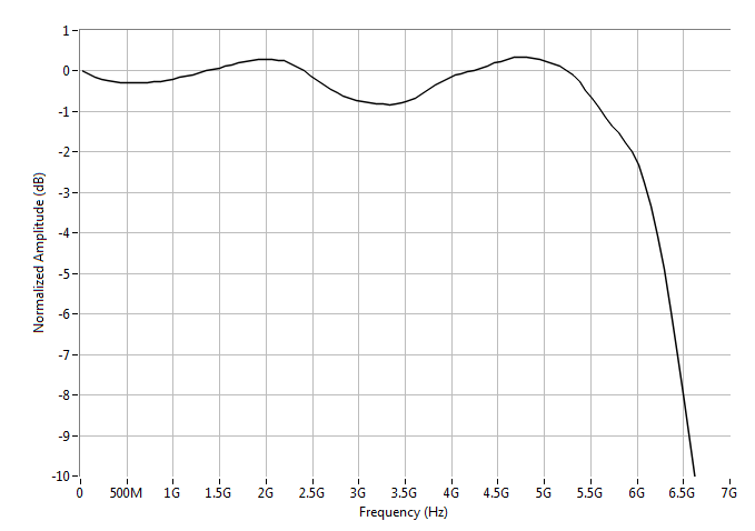
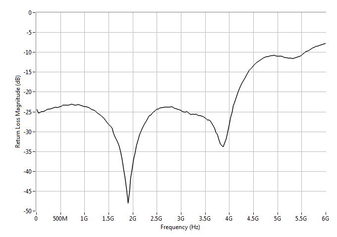
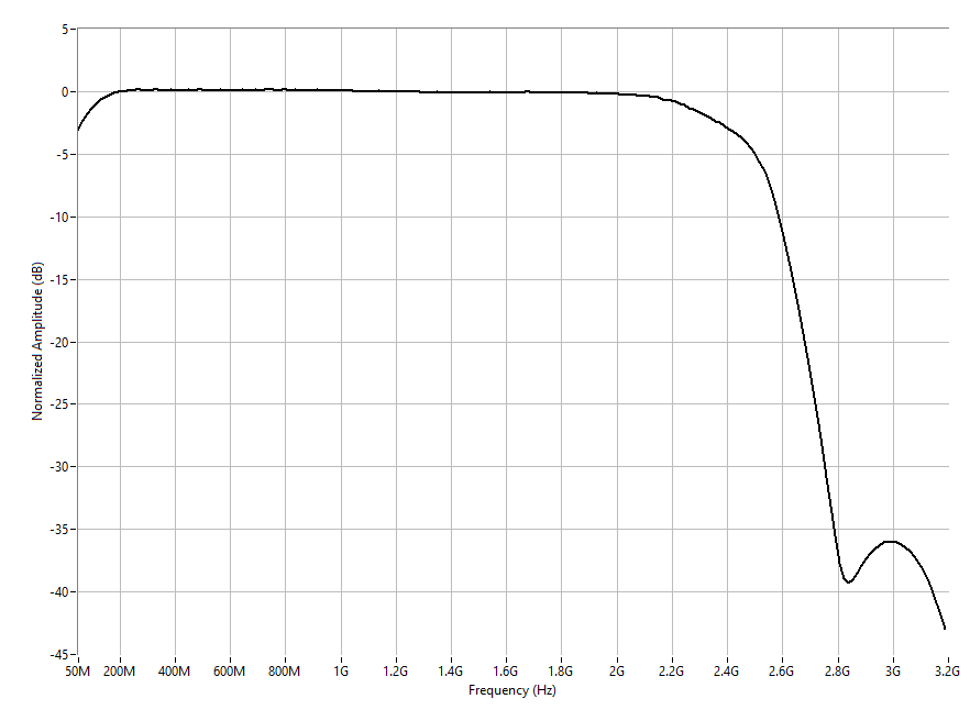
Analog Input
General Characteristics
Number of channels | 2, single-ended, simultaneously sampled | ||||||
Connector type | SMA | ||||||
Input impedance | 50 Ω | ||||||
Input coupling | AC | ||||||
| |||||||
| |||||||
Analog-to-digital converter (ADC) | ADC12DJ3200, 12-bit resolution | ||||||
239 ns | |||||||
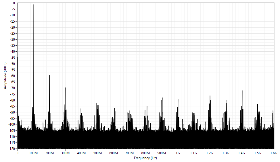
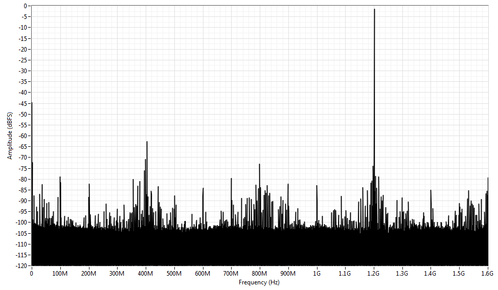
Typical Specifications
| Input Frequency | |||||
|---|---|---|---|---|---|
| 99.9 MHz | 399 MHz | 999 MHz | 1.999 GHz | 2.499 GHz | |
| SNR6 Measured with a -1 dBFS signal and corrected to full-scale. 3.2 kHz resolution bandwidth. [] (dBFS) | 56.0 | 55.6 | 54.7 | 52.9 | 51.6 |
| SINAD[] (dBFS) | 55.5 | 55.0 | 54.0 | 51.8 | 50.8 |
| SFDR (dBc) | -64.9 | -63.4 | -62.7 | -59.9 | -58.6 |
| ENOB7 Calculated from SINAD and corrected to full scale.[] (bits) | 8.9 | 8.8 | 8.7 | 8.3 | 8.1 |
| Input Frequency | |||||
|---|---|---|---|---|---|
| 99.9 MHz | 399 MHz | 999 MHz | 1.999 GHz | 2.499 GHz | |
| SNR[] (dBFS) | 54.6 | 54.2 | 52.4 | 49.7 | 48.9 |
| SINAD[] (dBFS) | 54.4 | 53.9 | 52.1 | 49.4 | 48.6 |
| SFDR (dBc) | -61.7 | -60.4 | -56.1 | -51.7 | -51.1 |
| ENOB[] (bits) | 8.7 | 8.7 | 8.4 | 7.9 | 7.8 |
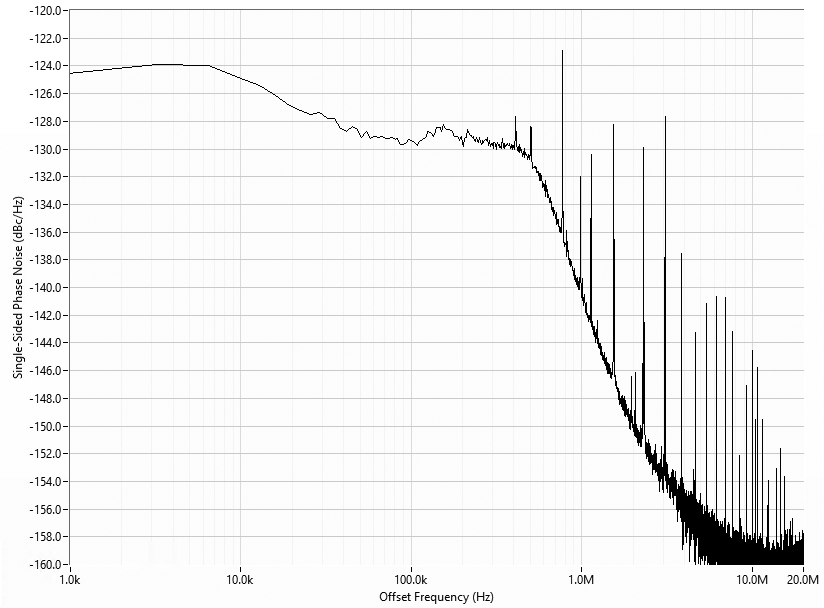
| Mode |
|
|
|
|---|---|---|---|
| Dual channel | 14.4 | -143.8 | -149.2 |
| Single channel | 9.8 | -147.2 | -152.6 |
| |||||||||||||
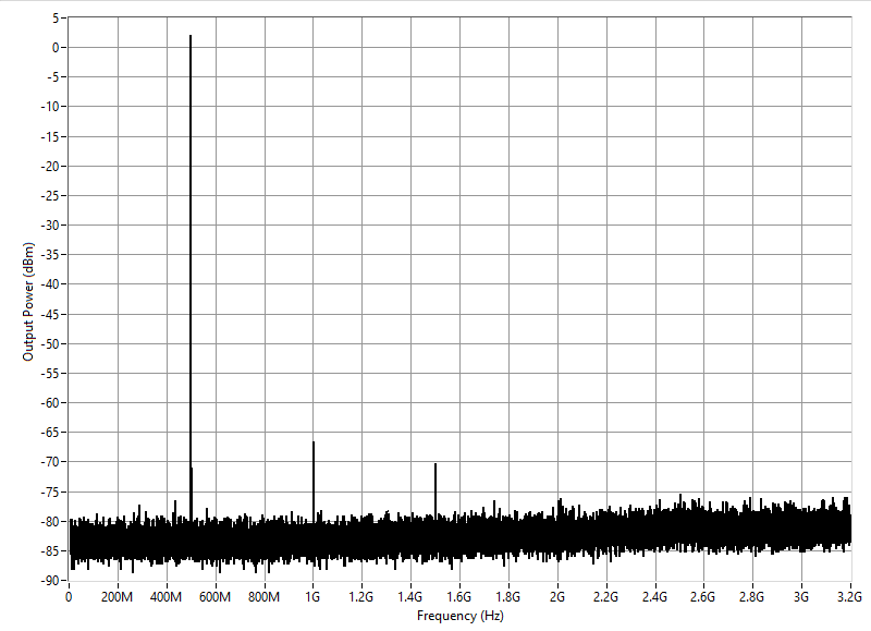
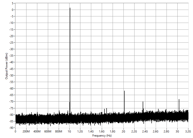
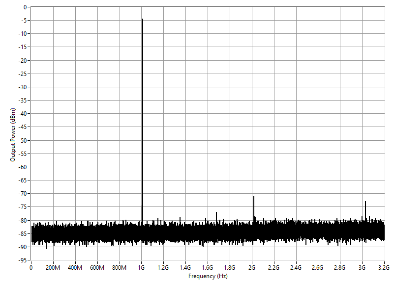
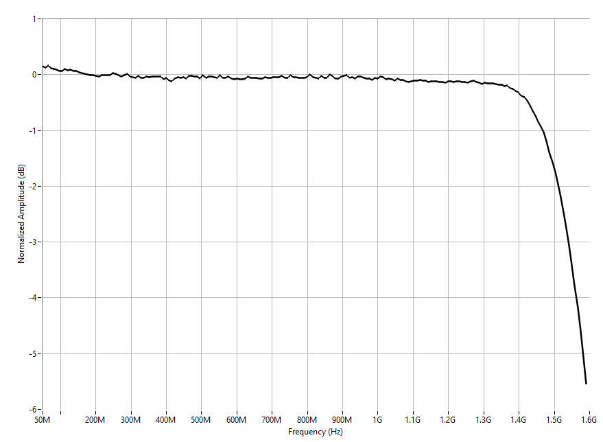
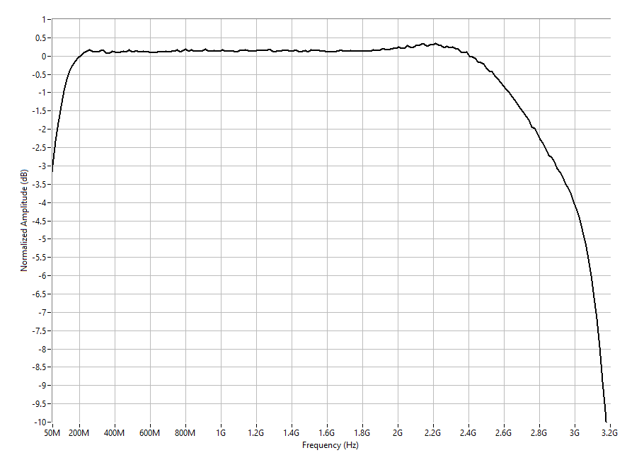
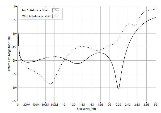
Analog Output
General Characteristics
Number of channels | 2, single-ended, simultaneously updated | ||||||
Connector type | SMA | ||||||
Output impedance | 50 Ω | ||||||
Output coupling | AC | ||||||
| |||||||
| |||||||
Digital-to-analog converter (DAC) | DAC38RF82, 12-bit resolution | ||||||
| |||||||
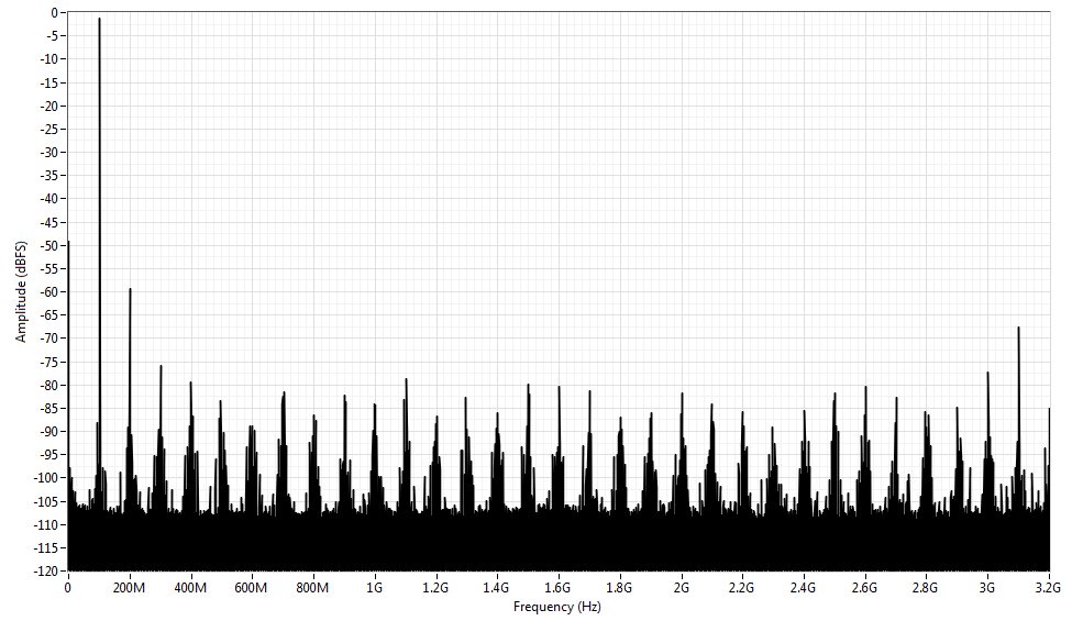
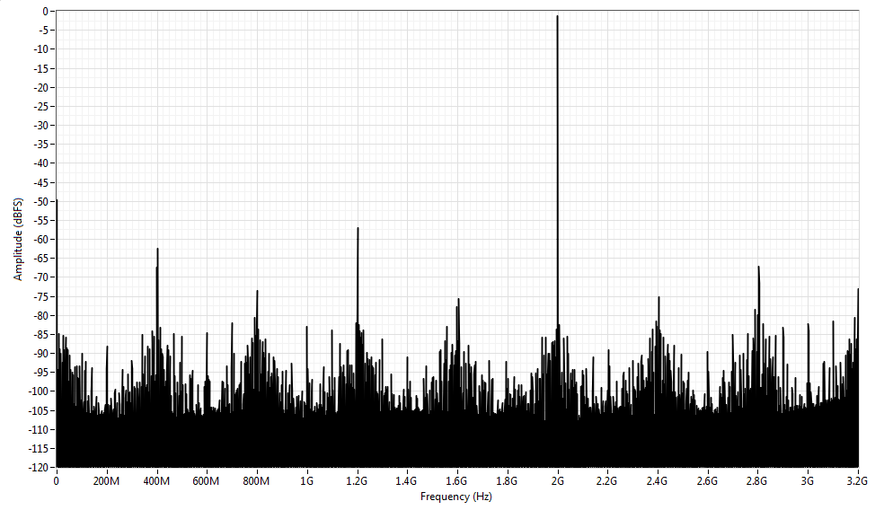
Typical Specifications
| |||||||||
| |||||||||
| Generation Frequency | ||
|---|---|---|
| 501 MHz | 1.01 GHz | |
| 2nd HD (dBc) | -67.8 | -61.7 |
| 3rd HD (dBc) | -63.0 | -62.0 |
| SFDR (dBc) | -63.0 | -61.7 |
| Generation Frequency | |
|---|---|
| 1.01 GHz | |
| 2nd HD (dBc) | -62.4 |
| 3rd HD (dBc) | -67.3 |
| SFDR (dBc) | -62.4 |
| Generation Frequency | ||
|---|---|---|
| 501 MHz and 511 MHz | 1.005 GHz and 1.015 GHz | |
| IMD3 (dBc) | -73.9 | -67.6 |
| 501 MHz Generation Frequency | |||
|---|---|---|---|
| Mode |
|
||
| Dual Channel | 1.18 | -165.5 | -168.4 |
| Single Channel | 0.941 | -167.5 | -164.2 |
REF/CLK IN
CLK/REF IN
Connector type | SMA | ||||||
Input impedance | 50 Ω | ||||||
Input coupling | AC | ||||||
Input voltage range | 0.35 V pk-pk to 3.5 V pk-pk, nominal | ||||||
Absolute maximum voltage | ±12 V DC, 4 V pk-pk AC | ||||||
Duty cycle | 45% to 55% | ||||||
| |||||||
| Clock Configuration | External Clock Frequency | Description |
|---|---|---|
| Internal PXI_CLK10[23]23 Default clock configuration. | 10 MHz | The internal Sample Clock locks to the PXI 10 MHz Reference Clock, which is provided through the backplane. |
| External Reference Clock (CLK/REF IN) | 10 MHz [24]24 The external Reference Clock must be accurate to ±25 ppm. | The internal Sample Clock locks to an external Reference Clock, which is provided through the CLK/REF IN front panel connector. |
| External Sample Clock (CLK/REF IN) | 2.8 GHz to 3.2 GHz | An external Sample Clock can be provided through the CLK/REF IN front panel connector. |
Bus Interface
Form factor | x8 PXI Express, specification v2.1 compliant |
Maximum Power Requirements
+3.3 V | 3 A |
+12 V | 4 A |
Maximum total power | 58 W |
Physical
Dimensions (not including connectors) | 18.8 cm × 12.9 cm (7.4 in. × 5.1 in.) |
Weight | 190 g (6.7 oz) |
Environment
Maximum altitude | 2,000 m (800 mbar) (at 25 °C ambient temperature) |
Pollution Degree | 2 |
Indoor use only.
Operating Environment
Ambient temperature range | 0 °C to 55 °C[25]25 The PXIe-5785 requires a chassis with slot cooling capacity ≥58 W. Not all chassis with slot cooling capacity ≥58 W can achieve this ambient temperature range. Refer to the PXI Chassis Manual for specifications to determine the ambient temperature ranges your chassis can achieve. (Tested in accordance with IEC 60068-2-1 and IEC 60068-2-2. Meets MIL-PRF-28800F Class 3 low temperature limit and MIL-PRF-28800F Class 2 high temperature limit.) |
Relative humidity range | 10% to 90%, noncondensing (Tested in accordance with IEC 60068-2-56.) |
Storage Environment
Ambient temperature range | -40 °C to 71 °C (Tested in accordance with IEC 60068-2-1 and IEC 60068-2-2. Meets MIL-PRF-28800F Class 4 limits.) |
Relative humidity range | 5% to 95%, noncondensing (Tested in accordance with IEC 60068-2-56.) |
Shock and Vibration
Operating shock | 30 g peak, half-sine, 11 ms pulse | ||||||
| |||||||
NI-TClk
You can use the NI-TClk synchronization method and the NI-TClk driver to align the Sample Clocks on any number of supported devices in one or more chassis. For more information about TClk synchronization, refer to the NI-TClk Synchronization Help within the FlexRIO Help. For other configurations, including multichassis systems, contact NI Technical Support at ni.com/support.
Intermodule Synchronization Using NI-TClk for Identical Modules
Synchronization specifications are valid under the following conditions:
- All modules are installed in one PXI Express chassis.
- The NI-TClk driver is used to align the Sample Clocks of each module.
- All parameters are set to identical values for each module.
- Modules are synchronized without using an external Sample Clock.
Skew[26]26 Caused by clock and analog delay differences. No manual adjustment performed. Tested with a PXIe-1085 chassis with a 24 GB backplane with a maximum slot to slot skew of 100 ps. Measured at 23 °C. | 80 ps, measured |
Skew after manual adjustment | ≤10 ps, measured |
Sample Clock delay/adjustment | 0.4 ps |
1 Multi-gigabit transceiver (MGT) signals are available on devices with KU040 and KU060 FPGAs only.
2 Voltage levels are guaranteed by design through the digital buffer specifications.
3 For detailed FPGA and High-Speed Serial Link specifications, refer to Xilinx documentation.
4 SMA input to LabVIEW diagram
5 Normalized to 10 MHz.
6 Measured with a -1 dBFS signal and corrected to full-scale. 3.2 kHz resolution bandwidth.
7 Calculated from SINAD and corrected to full scale.
8 Measured using channel AI0. Spectral performance may be degraded using channel AI1.
9 Excludes fixed interleaving spur (Fs/2 spur).
10 To achieve this update rate when using an external sample clock, inject a 3.2 GS/s clock into the REF/CLK IN port and enable 2x interpolation.
11 LabVIEW diagram to SMA output
12 Into a 50 Ω load.
13 Normalized to 10 MHz in dual channel mode and 200 MHz in single channel mode. 2x interpolation and inverse sinc filter enabled.
14 DC, 3.2 GHz, output corrected to 0 dBFS by inverse sinc filter, 2x interpolation, no anti-image filter.
15 2x interpolation, inverse sinc filter enabled, each tone corrected to -6 dBFS by inverse sinc filter.
16 Measured > 50 MHz offset from fundamental. 2x interpolation and inverse sinc filter enabled. Noise spectral density value depends on output tone frequency. See DAC38RF82 datasheet for noise spectral density results at other tone frequencies.
17 2x interpolation. Output corrected to 0 dBFS by inverse sinc filter. 10 kHz resolution bandwidth.
18 Aggressor channel generating a full-scale output into a 50 ohm terminator
19 -6 dBFS, 2x Interpolation, inverse sinc filter enabled, no anti-image filter, normalized to 200 MHz.
20 -6 dBFS, 2x Interpolation, inverse sinc filter enabled, normalized to 200 MHz.
21 Integrated from 3.2 kHz to 20 MHz. Includes the effects of the converter aperture uncertainty and the clock circuitry jitter. Excludes trigger jitter.
22 Integrated from 1 kHz to 30 MHz. Includes the effects of the converter aperture uncertainty, converter PLL circuitry, and the clock circuitry jitter. Excludes trigger jitter.
23 Default clock configuration.
24 The external Reference Clock must be accurate to ±25 ppm.
25 The PXIe-5785 requires a chassis with slot cooling capacity ≥58 W. Not all chassis with slot cooling capacity ≥58 W can achieve this ambient temperature range. Refer to the PXI Chassis Manual for specifications to determine the ambient temperature ranges your chassis can achieve.
26 Caused by clock and analog delay differences. No manual adjustment performed. Tested with a PXIe-1085 chassis with a 24 GB backplane with a maximum slot to slot skew of 100 ps. Measured at 23 °C.