PCIe-5764 Specifications
- Updated2025-04-24
- 9 minute(s) read
Definitions
Warranted specifications describe the performance of a model under stated operating conditions and are covered by the model warranty.
Characteristics describe values that are relevant to the use of the model under stated operating conditions but are not covered by the model warranty.
- Typical specifications describe the performance met by a majority of models.
- Nominal specifications describe an attribute that is based on design, conformance testing, or supplemental testing.
- Measured specifications describe the measured performance of a representative model.
Specifications are Typical unless otherwise noted.
PCIe-5764 Pinout

Digital I/O
Connector | Molex™ Nano-Pitch I/O™ |
5.0 V Power | ±5%, 50 mA maximum, nominal |
| Signal | Type | Direction |
|---|---|---|
| MGT Tx± <3..0>* | Xilinx UltraScale GTH | Output |
| MGT Rx± <3..0>* | Xilinx UltraScale GTH | Input |
| DIO <7..0> | Single-ended | Bidirectional |
| 5.0 V | DC | Output |
| GND | Ground | — |
| * Multi-gigabit transceiver (MGT) signals are available on devices with KU040 and KU060 FPGAs only. | ||
Digital I/O Single-Ended Channels
Number of channels | 8 |
Signal type | Single-ended |
Voltage families | 3.3 V, 2.5 V, 1.8 V, 1.5 V, 1.2 V |
Input impedance | 100 kΩ, nominal |
Output impedance | 50 Ω, nominal |
Direction control | Per channel |
Minimum required direction change latency | 200 ns |
Maximum output toggle rate | 60 MHz with 100 μA load, nominal |
| Voltage Family (V) | VIL (V) | VIH (V) | VOL (100 µA Load) (V) | VOH (100 µA Load) (V) | Maximum DC Drive Strength (mA) |
|---|---|---|---|---|---|
| 3.3 | 0.8 | 2.0 | 0.2 | 3.0 | 24 |
| 2.5 | 0.7 | 1.6 | 0.2 | 2.2 | 18 |
| 1.8 | 0.62 | 1.29 | 0.2 | 1.5 | 16 |
| 1.5 | 0.51 | 1.07 | 0.2 | 1.2 | 12 |
| 1.2 | 0.42 | 0.87 | 0.2 | 0.9 | 6 |
Digital I/O High-Speed Serial MGT
Data rate | 500 Mb/s to 16.375 Gb/s, nominal |
Number of Tx channels | 4 |
Number of Rx channels | 4 |
I/O AC coupling capacitor | 100 nF |
MGT TX± Channels
MGT RX± Channels
| |||||||
| Differential input resistance | 100 Ω, nominal |
| I/O coupling | DC-coupled, requires external capacitor |
Reconfigurable FPGA
PCIe-5764 modules are available with multiple FPGA options. The following table lists the FPGA specifications for the PCIe-5764 FPGA options.
| KU035 | KU040 | KU060 | |
|---|---|---|---|
| LUTs | 203,128 | 242,200 | 331,680 |
| DSP48 slices (25 × 18 multiplier) | 1,700 | 1,920 | 2,760 |
| Embedded Block RAM | 19.0 Mb | 21.1 Mb | 38.0 Mb |
| Default timebase | 80 MHz | ||
| Timebase reference sources | Onboard 100 MHz oscillator | ||
| Data transfers | DMA, interrupts, programmed I/O | DMA, interrupts, programmed I/O, multi-gigabit transceivers | |
| Number of DMA channels | 59 | ||
Onboard DRAM
Memory size | 4 GB (2 banks of 2 GB) |
DRAM clock rate | 1064 MHz |
Physical bus width | 32 bit |
LabVIEW FPGA DRAM clock rate | 267 MHz |
LabVIEW FPGA DRAM bus width | 256 bit per bank |
Maximum theoretical data rate | 17 GB/s (8.5 GB/s per bank) |
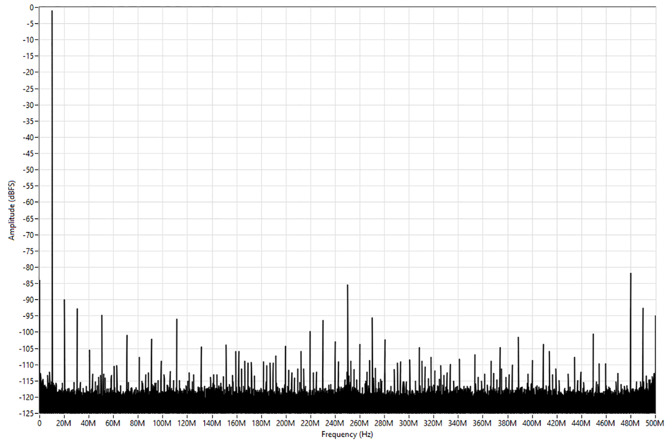
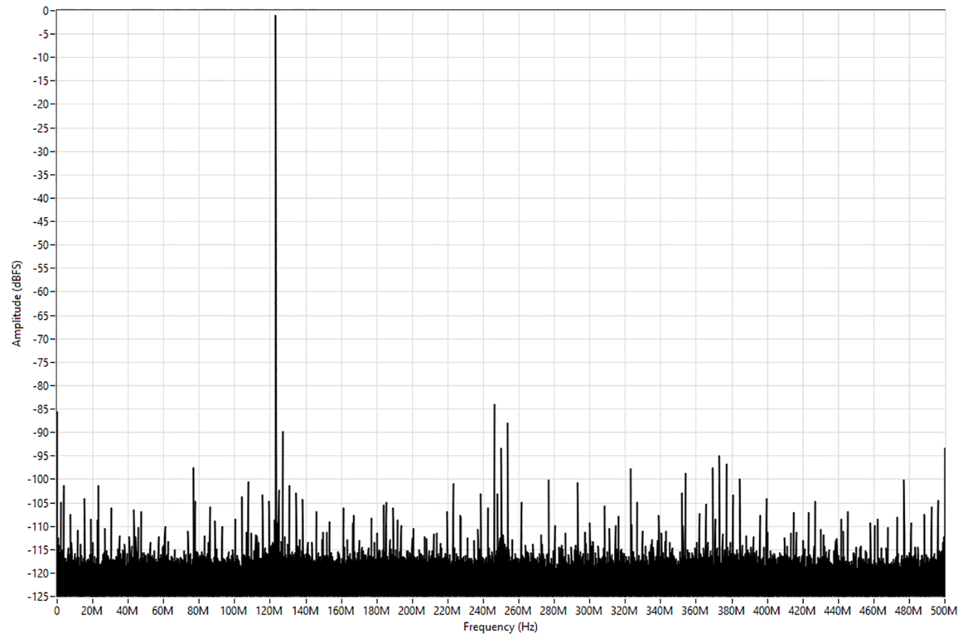
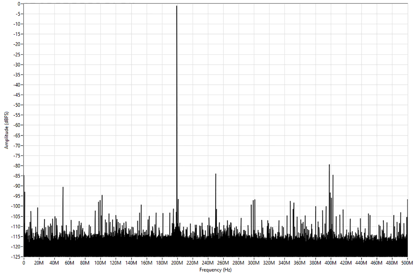
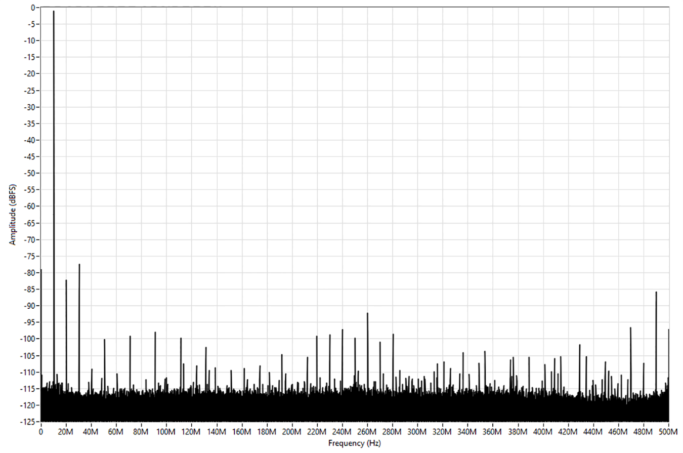
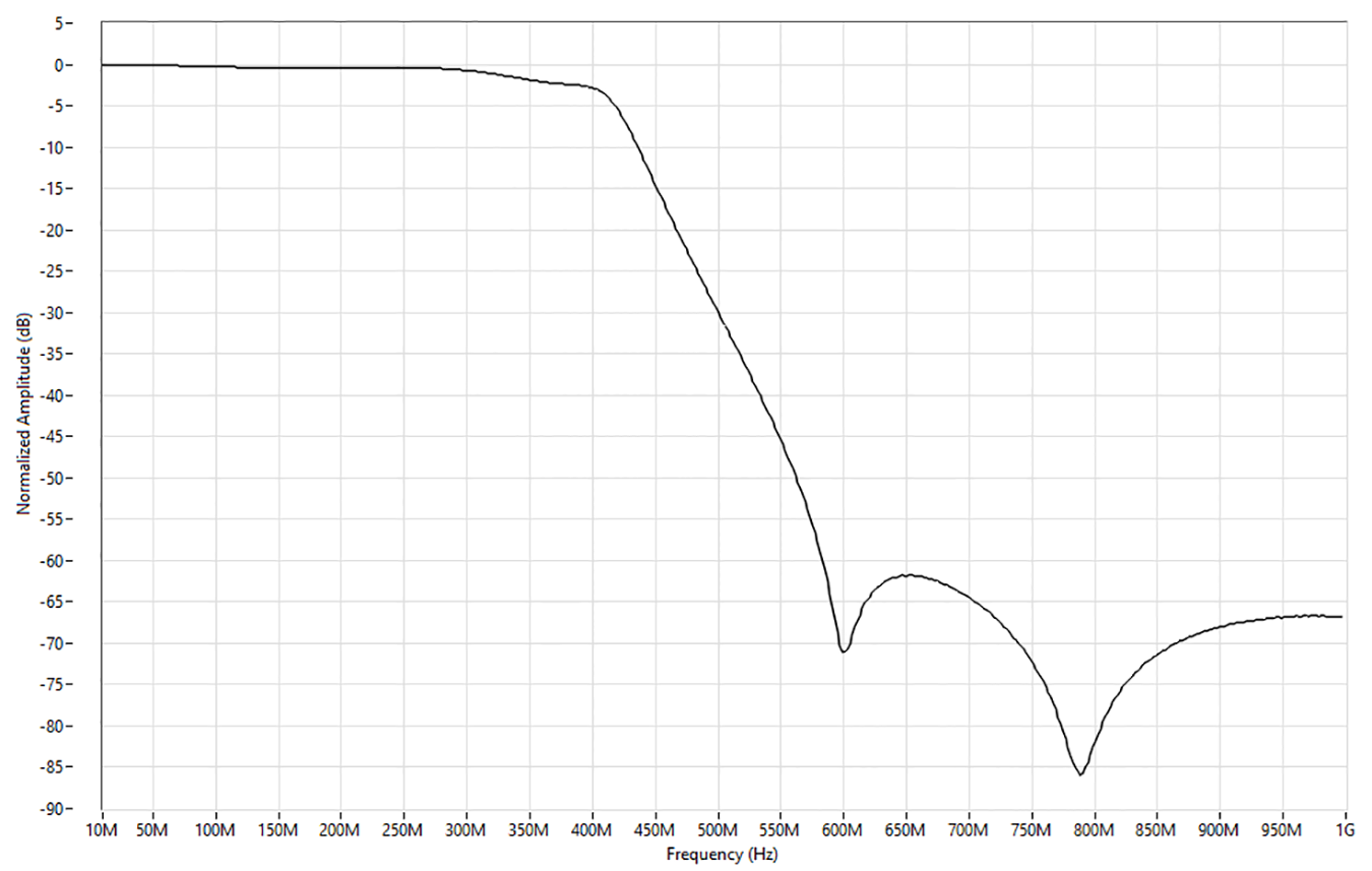
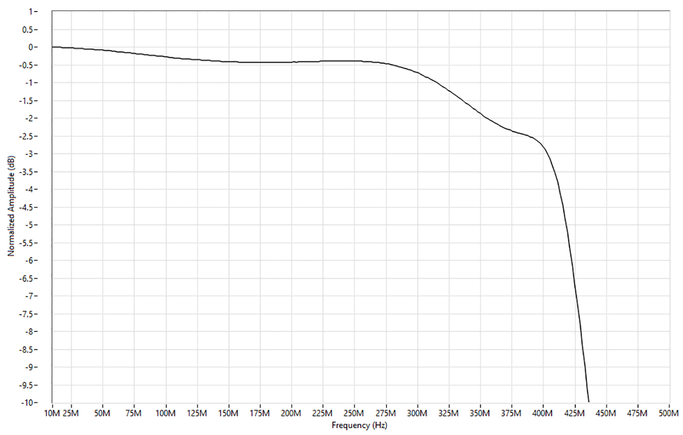
Analog Input
General Characteristics
Typical Specifications
| |||||||
| |||||||
| |||||||
| |||||||
| AC-Coupled | DC-Coupled | |||||
|---|---|---|---|---|---|---|
| Input Frequency | Input Frequency | |||||
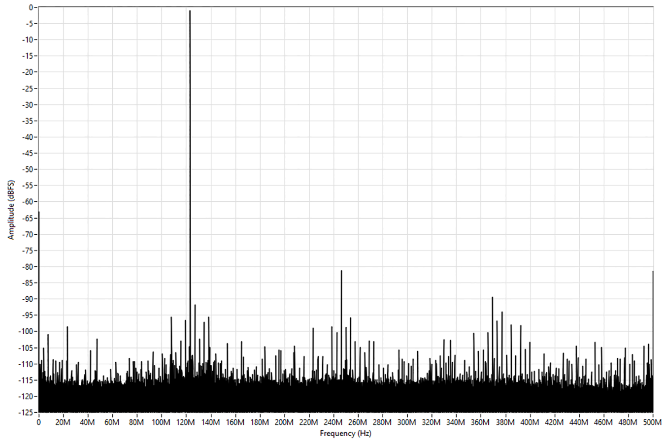
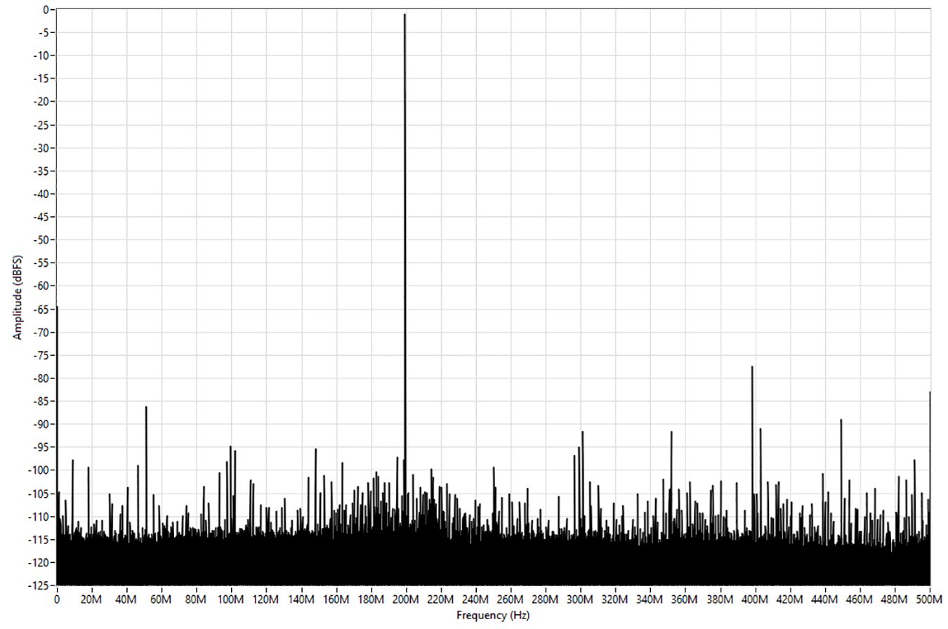
| 10.1 MHz | 123.1 MHz | 199.1 MHz | 10.1 MHz | 123.1 MHz | 199.1 MHz | |
| SNR* (dBFS) | 69.8 | 68.7 | 67 | 68.7 | 67.5 | 65.8 |
| SINAD* (dBFS) | 68.7 | 67.6 | 66.7 | 68.1 | 67.1 | 65.3 |
| SFDR (dBc) | -80.7 | -81.8 | -75.6 | -76.6 | -75.8 | -73.4 |
| ENOB† (Bits) | 11.1 | 10.9 | 10.8 | 11.0 | 10.9 | 10.6 |
|
* Measured with a -1 dBFS signal and corrected to full-scale. 1 kHz resolution bandwidth. † Calculated from SINAD and corrected to full-scale. |
||||||
| Module | nV/rt (Hz) | dBm/Hz | dBFS/Hz |
|---|---|---|---|
| AC-coupled | 9.7 | -147.3 | -157.5 |
| DC-coupled | 11.9 | -145.5 | -155.5 |
| |||||||||||
| |||||||||||
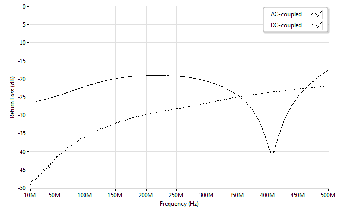
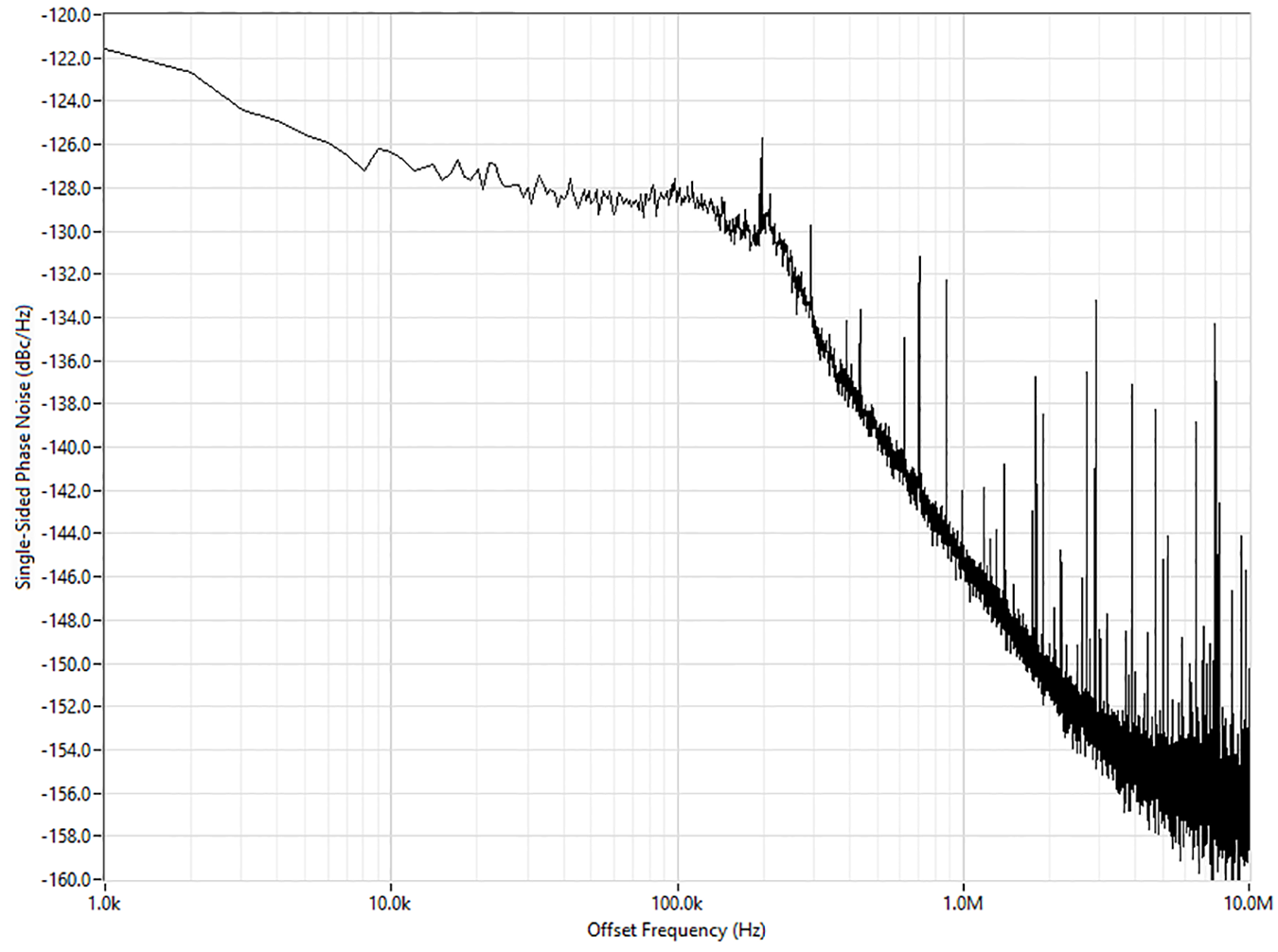
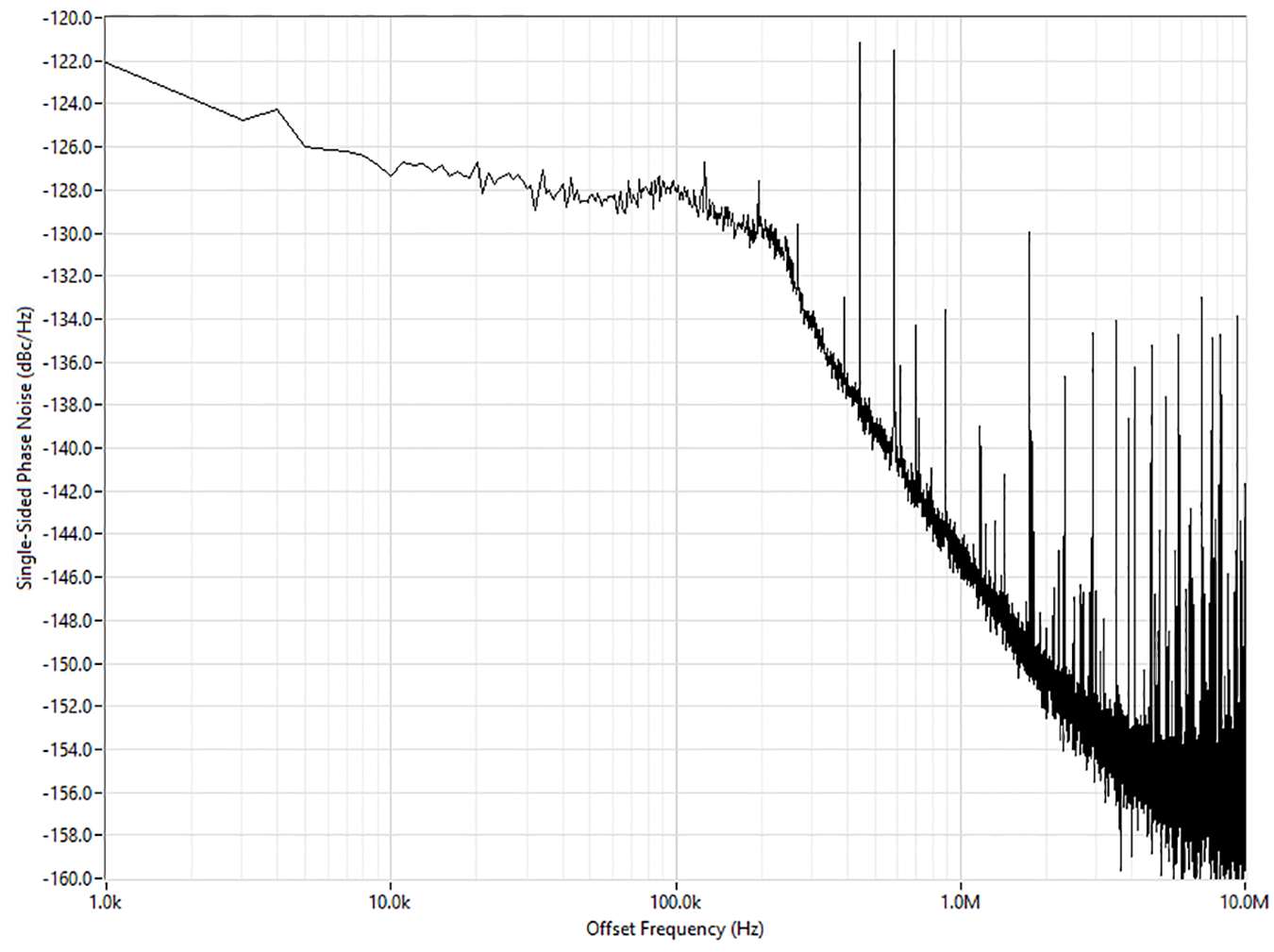
REF/CLK IN
General Characteristics
Connector type | SMA | ||||||
Input impedance | 50 Ω | ||||||
Input coupling | AC | ||||||
Reference input voltage range | 0.3 Vpp to 4 Vpp | ||||||
Sample Clock input voltage range | 0.3 Vpp to 4 Vpp | ||||||
Absolute maximum voltage | ±12 V DC, 4 Vpp AC | ||||||
Duty cycle | 45% to 55% | ||||||
Onboard reference timebase stability | ±0.7 ppm | ||||||
| |||||||
| Clock Configuration | External Clock Type | External Clock Frequency | Description |
|---|---|---|---|
| Internal Reference Clock* | — | — | The internal Sample Clock locks to an onboard voltage-controlled temperature compensated crystal oscillator (VCTCXO). |
| Internal Baseboard Reference Clock | — | 10 MHz | The internal Sample Clock locks to the 10 MHz Reference Clock provided from the FPGA baseboard. |
| External Reference Clock (REF/CLK IN) | Reference Clock | 10 MHz† | The internal Sample Clock locks to an external Reference Clock, which is provided through the REF/CLK IN front panel connector. |
| External Sample Clock (REF/CLK IN) | Sample Clock | 1 GHz | An external Sample Clock can be provided through the REF/CLK IN front panel connector. |
|
* Default clock configuration. † The PLL Reference Clock must be accurate to ±25 ppm. |
|||
Bus Interface
Card edge form factor | PCI Express Gen-3 x8 |
Slot compatibility | x8 and x16 PCI Express |
Maximum Power Requirements
+3.3 V | 4.5 A |
+12 V | 5 A |
Maximum total power | 75 W |
Physical
Dimensions (including I/O bracket, not including connectors) | 12.6 cm × 26.3 cm × 4 cm (5.0 in. × 10.4 in. × 1.6 in.) |
Weight | 990 g (35 oz) |
PCI Express mechanical form factor | Standard height, three-quarter length, double slot |
Integrated air mover (fan) | Yes |
Maximum rear panel exhaust airflow | 84 m3/h (50 CFM) (without any chassis impedance) |
Environment
Maximum altitude | 2,000 m (800 mbar) (at 25 °C ambient temperature) |
Pollution Degree | 2 |
Indoor use only.
Operating Environment
Operating temperature, local[7]7 For PCI Express adapter cards with integrated air movers, NI defines the local operational ambient environment to be at the fan inlet. For cards without integrated air movers, NI defines the local operational ambient environment to be 25 mm (1 in.) upstream of the leading edge of the card. | 0 °C to 45 °C |
Operating humidity | 10% to 90% RH, noncondensing |
Storage Environment
Ambient temperature range | -20 °C to 70 °C |
Relative humidity range | 5% to 95% RH, noncondensing |
1 Voltage levels are guaranteed by design through the digital buffer specifications.
2 800 mV peak-to-peak when transmitter output swing is set to the maximum setting.
3 Only one analog input path type is populated.
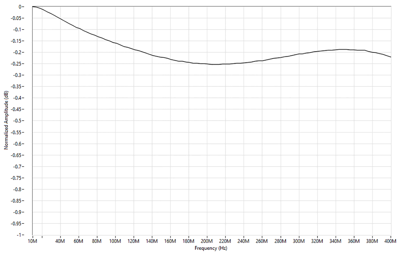
4 Normalized to 10 MHz.
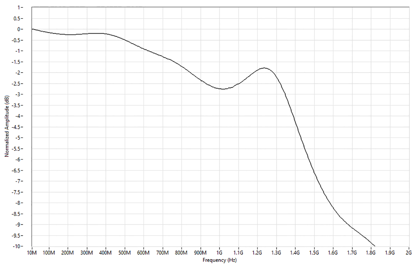
5 Maximum bandwidth for full scale input signal is 400 MHz. See the ADS54J60 datasheet for details on maximum supported amplitude for frequencies greater than 400 MHz.
6 Integrated from 1 kHz to 10 MHz. Includes the effects of the converter aperture uncertainty and the clock circuitry jitter. Excludes trigger jitter.
7 For PCI Express adapter cards with integrated air movers, NI defines the local operational ambient environment to be at the fan inlet. For cards without integrated air movers, NI defines the local operational ambient environment to be 25 mm (1 in.) upstream of the leading edge of the card.