Three Steps to Using DRAM Effectively on FPGA Devices
Overview
There are three primary design considerations that can have a dramatic impact on the throughput and storage capacity obtainable from the dynamic random access memory (DRAM) interface on FPGA devices:
1. Access Size and Frequency
2. Request Pipelining
3. Sequential Access
Contents
- Access Size and Frequency
- Request Pipelining
- Sequential Access
- Additional Resources
- Appendix: Bandwidth and Latency
Access Size and Frequency
To optimize DRAM throughput, data must be sized properly and data must be written to DRAM at the correct clock rate.
Access size describes the internal representation of data in the memory; it is the amount of information that is stored in one memory address. You can set up memory items to use a variety of data types; however, to achieve the best performance, use a data type that matches the device’s access size. The access size is the exact number of bits that are written/read in a given memory access. If you use a data type that is smaller than the access size, the remaining bits receive an unknown and invalid value, but still get written and take up both space and bandwidth.
Each FPGA module family has its own access size to optimize throughput without considerably increasing the clock rate at which the memory interface needs to execute. The table below shows the main specifications for the DRAM in each FPGA module family, including the access size that the memory expects.
| Module | Number of DRAM Banks | Size per Bank | Bandwidth per Bank | Access Size | Optimal Clock Rate |
|---|---|---|---|---|---|
| PXIe-782xR | 1 | 512 MB | 800 MB/s | 64 bits | 100 MHz |
| PXI-795xR | 2 | 64 MB | 800 MB/s | 64 bits | 100 MHz |
| PXIe-796xR | 2 | 256 MB | 1.6 GB/s | 128 bits | 100 MHz |
| PXIe-797xR | 1 | 2 GB | 10.5 GB/s | 512 bits | 166 MHz |
| cRIO-903x | 1 | 128 MB | 1.6 GB/s | 128 bits | 100 MHz |
Note: The PXIe-7820R, PXI-7951R, PXIe-7961R, and PXIe-7971R do not have DRAM.
To achieve maximum throughput, NI recommends using data types that are the same width as the access size of the device that is being targeted to ensure that each access is fully utilized. Clusters can be used to easily package data into packets that are the correct aggregate size.
Optimizing access size alone, though, isn’t enough to maximize bandwidth. To maximize bandwidth, data must also be pushed into DRAM at the optimal clock rate. For example, an PXI-7954R pushing 64 bits into DRAM at a rate of 100 MHz is pushing 8 bytes * 100 MHz = 800MB/s, and a PXIe-7966R achieves twice as much data from a 100 MHz clock because the data width is doubled to 16 bytes/clock. Therefore, writing data to DRAM in a clock domain less than the optimal clock rate does not take full advantage of the available bandwidth. This may or may not be acceptable depending on the application.
Request Pipelining
DRAM is built on a highly pipelined architecture, and therefore has a certain amount of latency between requests for data and the actual execution of that request. By pre-requesting samples, you can maintain high throughput. The figure below illustrates two possible strategies for accessing DRAM. In waveform (a), you request data (issue Read command), and then wait for it to show up in the Retrieve method (strobe is asserted). This strategy does not take advantage of the memory’s internal pipelining, so the throughput is limited by the DRAM’s latency.
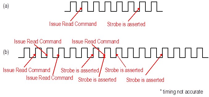
Instead, architect your design with the “look ahead” approach illustrated in (b). In this method, you keep requesting the data you wish to read without waiting for the Retrieve method to return data. The requests for reads and writes get stored in a queue inside the memory item and then passed on to the memory controller, which also has an internal queue where it picks out commands in order. Even though each individual request is still subject to latency and some non-determinism, you now get much higher throughput rates because DRAM can access several pieces of data sequentially instead of treating each request separately.
Sequential Access
DRAM is optimized for high storage density and high bandwidth. One assumption DRAM designers make is that data will be accessed sequentially in ascending order, that is, you read the data in address 0x1 after you read the data in address 0x0. Another assumption is that data will be accessed in big blocks. Both of these assumptions are true in modern PC architectures. The processor reads big blocks of memory into cache, even if the program being executed requested a single byte. For instrument designers, this means avoiding jumping back and forth between reading and writing, as well as between noncontiguous addresses, and avoiding writing the memory in a decrementing-address fashion.
In theory, the most efficient access strategy is to do only one type of access (either read or write) on a large number of sequential addresses. However, this is not practical. Memory that you write to but never read from, for example, is not useful. Instead, you should try to maximize the amount of sequential data that you access. You can switch between access types and addresses, but you will be most efficient if you don’t do it often and if you access big blocks of data (hundreds of elements) between jumps.
Note: Follow best practices for out of range accesses. Reading or writing to addresses beyond the size of your memory block can have very confusing behavior. Always be mindful of how many elements are allocated to your memory block. By enabling error terminals on your memory methods, you can detect out of bounds memory accesses.
Additional Resources
- Because optimal DRAM access patterns for read-write interfaces can be difficult to create, the NI FlexRIO Instrument Development Library provides open LabVIEW and LabVIEW FPGA VIs implementing these patterns, in addition to record- and waveform-based memory segmentation.
- Explore an introduction to using DRAM with NI FPGA Devices
- Learn more about FlexRIO
- Learn more about R Series Devices
- Learn more about CompactRIO
Appendix: Bandwidth and Latency
Bandwidth and latency are two important topics to review. Bandwidth refers to the maximum amount of data that can be transferred per unit time, or how many bytes you can write to/read from the memory in a second. Latency refers to the amount of time that elapses between requesting a piece of data from the memory and when you actually receive it.
DRAM is designed to provide high storage density and high bandwidth. Modern DRAM interfaces can transfer vast amounts of data per unit of time. For instance, the PXIe-7976R FlexRIO FPGA Module has a single DRAM bank with 10.5 GB/s of bandwidth, giving the PXIe-7976R the ability to store data at a rate of 10.5 GB/s, considerably faster than the PCI Express bus connecting the module to the host processor. DRAM achieves this bandwidth by using a highly pipelined architecture. This means that DRAM performs best when transferring large blocks of data to or from sequential addresses. The latency of DRAM, however, is relatively large compared to that of the built-in block RAM in the FPGA, easily taking tens of clock cycles to complete an access operation.