Accurate Switch-Mode-Power-Supply Designs with NXP Components
Overview
Contents
- Introduction
- Application Example: Medium Power DC-DC Buck Converter Using the Improved Technology of low VCEsat Transistors
- Design Specifications
- Circuit Set-up
- Simulation and Analysis
- Efficiency and thermal behavior
- Conclusion
Introduction
National Instruments and NXP work closely together to provide a complete set of discrete component models within a powerful simulation environment. The combination of accurate models and intuitive simulation tools enable the designer to accurately evaluate circuit performance prior to prototyping leading to an enhanced design performance, reduced design errors and ultimately fewer prototype iterations. 1,500+ NXP discrete components have been added to the NI Multisim 13.0 component library. The components include SPICE models for simulation as well as ready-to-use footprints for rapid layout in NI Ultiboard.
This document highlights how Multisim is used for vital calculations in a design using switch mode power supplies (SMPS). Performance metrics reviewed include transient response, steady-state ripples, power efficiency and thermal characteristics.
Application Example: Medium Power DC-DC Buck Converter Using the Improved Technology of low VCEsat Transistors
This example demonstrates simulation of the power stage of a DC-to-DC buck converter using NXP models. Simulation is used to make accurate design decisions that directly impact circuit performance, including:
- Choosing capacitor and inductor values to meet ripple requirements
- Choosing gate driver components to ensure that the BJT is driven optimally
- Calculating the efficiency of the converter
- Calculating power dissipation to gain insight about the thermal behavior
Design Specifications
The design needs to meet the following conditions and design requirements:
| Condition | Value |
| Input voltage | 10V |
| Equivalent load resistance | 2Ω |
| Switching Frequency | 50kHz |
| Design Requirement | Value |
| Output voltage | 3.3V |
| Inductor current ripple | <400mA |
| Output voltage ripple | <60mV |
| Efficiency | >80% |
This application is suitable for the low VCEsat products by NXP because it is optimized for high-speed switching. The high and constant current gain, the low saturation voltage and the good switching performance of NXP BISS-4 transistors allow the use of a bipolar transistor for the described medium-power DC-to-DC converter instead of a P-channel MOSFET.
The BISS transistor proposed in the example is optimized for minimized switching times. The storage and switching times are much reduced compared to types optimized for an ultra low VCEsat.
Circuit Set-up
As a first pass, based on the operating voltage current (10V, 1.65A), we choose the PBSS4032PD PNP transistor (30V, 2.7A) as the main switch and the PMEG3020BEP Schottky diode (30V, 2A) as the freewheeling diode.
To help manage and choose values for the various parameters in the circuit, we use the circuit parameter feature to define key parameters that will be critical to the device performance. These device parameters are variable and will dynamically determine the inductor and capacitor values. As seen in the circuit parameters window certain values such as Vin, Fsw and Vout have been set to specific static values. Other values such as L and C are dependent on mathematical expressions that include Vin, Vout etc…. This is shown in the table to the left.
To learn more about circuit parameters click here.
Parameters Duty, L, and C are all calculated dynamically from other parameters. The formulas for these parameters are based on fundamental equations of an ideal buck converter and provide a reasonable starting point for choosing values. The Preview column provides the numerical evaluation of the expression. We apply certain circuit parameters, including L and C, directly to values of component parameters in our buck converter circuit.
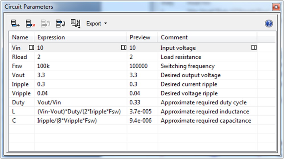
Figure 1. Circuit Parameters table in Multisim
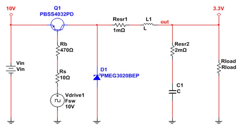
Figure 2. Circuit topology of the buck converter
Simulation and Analysis
A 1ms transient analysis simulation quickly generates the following waveforms for the output voltage and inductor current in Figure 3.
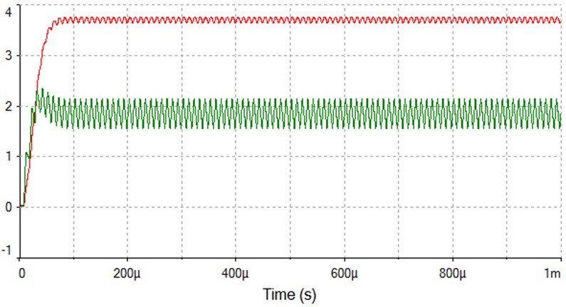
Figure 3. Transient response of the circuit using the initial component values.
Note that the output voltage, at 3.7V (shown in red in Figure 3), is inconsistent with expectations from theoretical calculations. As a result of the various voltage drops across the BJT and the diode, the expectation is to see a voltage slightly lower than 3.3V, not higher. But on inspection of the BJT waveforms with respect to the drive signal we can see the cause in Figure 4.
The actual BJT turn-on and turn-off events (in green) lag the gate drive signal significantly. The turn-off lag is greater than the turn-on lag, explaining the higher-than-expected output voltage.
By using this simulation of the performance we also uncover a far more serious problem that the BJT spends a significant amount of time in the active region where it consumes a large amount of power. Probing the average power dissipation in the BJT results in 2.5W of power dissipation. This implies not only that the efficiency of the converter is likely below 50% but also that the transistor will probably be destroyed without an impractically large heat-sink
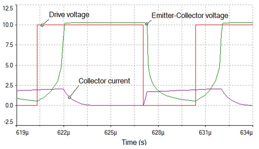
Figure 4. Switching transistor current and voltage waveforms
Luckily this problem can be easily mitigated by placing a small capacitor in parallel with the base resistor as shown in Figure 5.
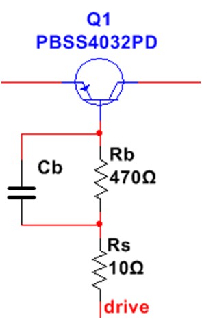
Figure 5. Capacitor Cb added to the base resistance to reducedelay
This capacitor provides extra current during the turn-on and turn-off transients.
We performed a simple parameter sweep analysis to determine a good value for the capacitor. We have chosen the power dissipated by the transistor as the metric for evaluating the effectiveness of various capacitor values. The following graph shows the average power dissipation of the transistor for various values of the capacitor. From a range of 1pF to 1uF, a value of 10nF appears to provide turn-on/turn-off characteristics that result in the lowest power dissipation. A more standard value for the capacitor, 4.7nF, yields the following results for the output voltage and inductor current.
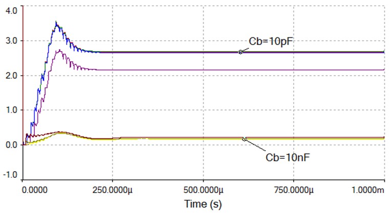
Figure 6. Results of the parameter sweep simulation over the value of Cb
The output voltage, at 3.1V, is now much more in-line with our expectations. In practice this converter would be operated at a duty cycle higher than 33% to compensate for the various voltage drops which pushes the output voltage below the value expected from the ideal relationship, Duty*Vin.
The inductor current ripple is 298mA, which matches our estimate from the ripple formula, and is below the required maximum.
The voltage ripple evaluated in Figure 7 is 60mV, which is higher than that expected according to the ripple formula; it is also just at the limit of the requirement. The excess ripple is a result of the output capacitor’s ESR. It is preferable to reduce it.
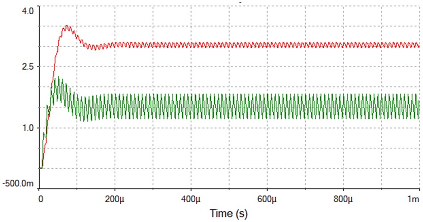
Figure 7. Transient time response of the circuit topology after adding Cb
Simulation provides an interesting insight into the sensitivities of the ripple. For instance increasing the capacitance value from 9.4uF to 100uF reduces the ripple only by 5mV. However it also shows that decreasing the ESR from 200mΩ to 100mΩ reduces the ripple by 15mV. Therefore it may be more effective to decrease the ESR rather than increase capacitance to reduce ripple in our circuit.
Efficiency and thermal behavior
Now that we are able to properly drive the BJT and have met the ripple requirements, we can turn our attention to the efficiency of the converter and its thermal behavior.
The efficiency of the converter is calculated by setting up the following output expression in Multisim:
-1*avgx(P(RLOAD),60e-6)/avgx(P(VIN),60e-6)
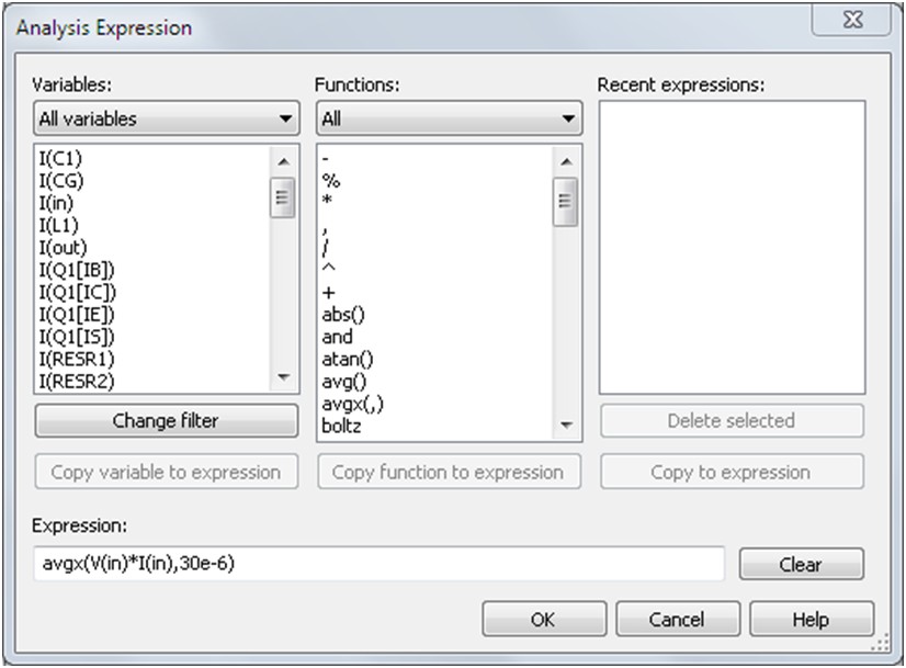
Figure 8. Adding expressions to a simulation setup in Multisim
The expression divides the 60us running averages of the power dissipated in the resistor by the power dissipated in the input voltage source. The “-1” is used to provide a positive number since the reference for power is dissipative. The following plot shows the result of this expression along with the major contributors to overall power dissipation - the Diode and BJT.
An efficiency of 87% meets the requirements. However it should be possible to improve the efficiency of the converter by, for instance, selecting different BJT and Diode components. Since many other fully functional NXP components are readily available in the Multisim database, attempting to optimize the design by swapping in and out different components is simple.
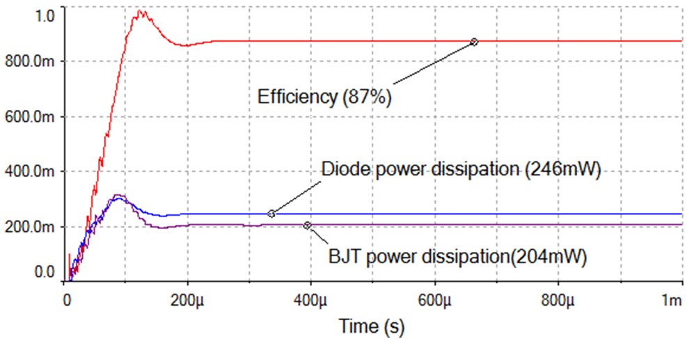
Figure 9. Power dissipation and efficiency calculation in Multisim
The average power dissipation provides insight about the thermal behavior of the components, the junction temperature in particular. For instance, from the datasheet of the PBSS4031PD, we note that the thermal resistance from junction to ambient for a BJT mounted on an FR4 board on a 6cm2 mounting pad is 160°/W. With an average power dissipation of 204mW, the average junction temperature rise above ambient is 0.205*160=32.8°. Therefore, there is plenty of headroom before the junction temperature reaches the maximum temperature of 150°.
Conclusion
This note showed how Multisim could be used to quickly determine key parameters of a DC-DC converter. The converter is based on the new low VCEsat transistor models and diode parts from NXP. The design of the BJT-based converter is properly driven and meets ripple and efficiency requirements, while determining power dissipation of the switching elements helped better understand the contributors to the losses and the implications on the thermal design.
NI and NXP continue to offer circuit designers a complete library of accurate component models and a simulation environment that enables them to evaluate their circuit performance resulting in a more efficient flow and improved prototype designs.