Generating and Debugging Constraints for High Speed Serial Instruments
Overview
Contents
- What are Constraints?
- Why are Constraints Required for my Project?
- What Process Exists for Developing a NI High Speed Serial Design?
- How are Constraints Generated?
- Design Hierarchy in LV FPGA and the CLIP
- Best Practices for Generating Constraints
- Common Issues and Troubleshooting
- Aurora IP Constraints Overview
- References
What are Constraints?
Figure 1: Example Constraints for NI’s Aurora Sample Project
Working on a new FPGA design, you will ultimately come to the point where you need to compile your design for testing, to determine if the design meets compilation timing and placement requirements, as well as functional requirements. Constraints are a way to inform the compiler of specific placement and timing requirements needed in order to achieve a successful compilation. In essence, you are instructing the compiler to change the way it designs and analyzes your code in order for it to create a valid and functional bitstream.
Most often, these constraints are broken down into four main categories: timing assertions, timing exceptions, physical locations, and synthesis-level constraints. For your High Speed Serial Instrument project, timing assertions and exception constraints will be the main focus for what you need to add or modify. Timing assertions are often related to clocking, while timing exceptions detail the input signal arrival times, output signal required times, false paths, and max delays.
Why are Constraints Required for my Project?
Figure 2: Compilation Error and Compilation Success Indicators
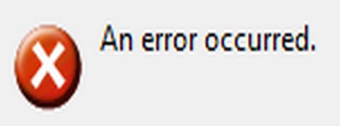

The requirement for constraints in your project comes down to timing closure, successfully interfacing to high performance I/O, and achieving successful compilations of your project. Since FPGA design is very open to interpretation, and no two compilations are the same, the compiler works to identify the best routing for the design you have created inside the FPGA given known timing requirements for the specific project. Adding constraints allows the compiler to understand where it should be “extra” careful when routing signals, or where it should ignore timing on asynchronous timing paths, or how it should interpret different design techniques that you choose to use. All of this adds up to creating a successful FPGA design which is functional and meets application requirements.
Ideally, you will be able to identify constraints that you will need as you begin creating your design. For a first time user, this may be difficult to do without some understanding of why constraints are a requirement for the project. Not using constraints could lead to failing compilations even though the design has no need for changes. Even more dangerous, a lack of constraints could lead to a compilation passing compilation, but not meet timing required to ensure functional operation. It is best to avoid this situation by fully understanding the requirement for constraints and forming them correctly in your project.
What Process Exists for Developing a NI High Speed Serial Design?
Understanding the process of developing a High Speed Serial project, from the very beginning of inception all the way through a successful bitstream running on your instrument will help you efficiently develop and complete your design successfully. Below are a few flow charts to help you understand the typical design flow, and where generating constraints come into your design:
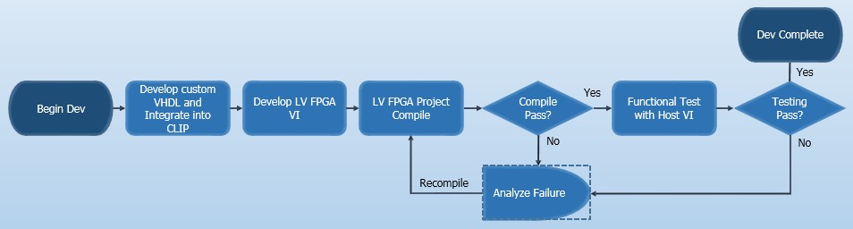
- Begin development by developing custom VHDL or skip this step if you are using an example IP core from a 3rd party vendor. Integrate VHDL that you wish to use in your application into a top level Component Level IP (CLIP) which will be used by your High Speed Serial instrument. Refer to previous examples provided by NI and help documentation to understand this process.
- Once the CLIP is created, add it into your LV FPGA project and develop the LV FPGA VI which interfaces to the CLIP and the Host. This may involve adding AXI compliant interfaces, FIFOs for data flow, and algorithms to perform on your data in the FPGA. Refer to NI examples and User Manual documentation to understand typical functionality in this VI.
- Once the LV FPGA VI is developed for your project, create a Build Specification and compile your full design. Note: there are some project configuration steps that are not detailed here that you will need to check and configure to successfully compile.
- If the compile passes, proceed to functionally test the successful LV bitfile on the High Speed Serial instrument. If the compile fails, proceed to analyzing the failure and then recompile when you have corrected any errors encountered. Refer to the flow chart below on typical debugging steps for failed compilations.
- If functional testing shows your bitfile behaves like you’d expect, you now are dev complete on your overall design. Otherwise, continue adding features and going through the process again for new updates to your design.
When analyzing compilation failures in your design, refer to the flow chart below. This process will most likely be performed several times as you iterate through various errors you encounter while developing.
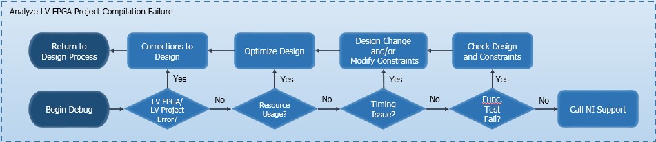
- If your compilation fails due to LV FPGA or LV Project errors, correct those errors listed and recompile the design.
- If your compilation fails due to resource utilization, optimize the design to use less resources.
- If your compilation fails due to timing violations, your design may require additional design changes and/or you need to apply correct timing constraints to inform the compiler on how to handle certain timing violations.
- After functionally testing successfully compiled IP, if you find inconsistent behavior, you will need to go over the design to look for any errors in logic, and/or ensure all paths that are timing sensitive are constrained properly.
You will notice that during compilation failures, you may for the first time discover the need to generate constraints in your project. This document will detail that process and give best practices for generating constraints.
How are Constraints Generated?
There are several methods for generating constraints for a particular High Speed Serial Instrument design. You will likely need to manually create an .xdc file with your design constraints. To help you with this process, there are pre-existing constraints from examples that come from Xilinx, NI, or 3rd parties that you can pull into your projects .xdc file. Designing with NI High Speed Serial, LV FPGA will also generate constraints based on certain selections that you make in your LV FPGA project. Finally, there are other tools provided by Xilinx that can help generate constraints, such as Vivado Constraint Editor.
3rd Party Examples
When you are developing your design for your High Speed Serial Instrument, you will often start from an example design, or use an IP core that you are integrating into the design in order to communicate using a particular protocol. Several 3rd parties provides many different IP cores that can be used to instantiate a specific protocol communication interface in your design. Xilinx also provide IP cores in Vivado that you may start developing from.
With these cores, there are Example Designs which show how the IP core is used in a successfully compiled design that can be loaded onto an FPGA. The Example Design may contain several .xdc files which may be utilized to help constrain your design.
Figure 3: Vivado Project Manager Showing .xdc Constraint File
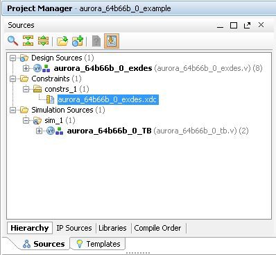
Inside the .xdc file is a list of Tcl commands which apply the constraints during compilation.
Figure 4: .xdc Constraint File Example
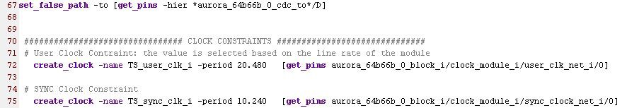
The constraints in this example file can be copied to your design (with some modification) based on where the clocks reside in your particular CLIP and hierarchy. There will be more on this conversion later in this paper.
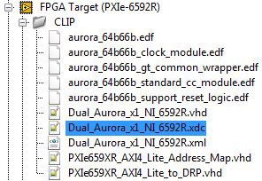
NI Examples
You can also see with NI Examples that we have provided a completed XDC constraints file to include with your project. You can find this in our example project window under the CLIP folder:
Figure 5: .xdc File Contained in CLIP Folder inside LV FPGA Target
Manually Generate Constraints
Using industry standard Synopsys Design Constraints (SDC) format, a user can create timing assertions and timing exceptions on their own with any text editor program. This method requires an understanding of the constraint syntax and knowledge on how to successfully locate pins, ports, and cells in a design. It is best at first to start from an example design before attempting this method.
Nearly every High Speed Serial project will require some level of manually editing the .xdc to be successful. It is important to understand the tools you have available to you to help create the .xdc file and to also understand which constraints are created for you in LV FPGA.
LV FPGA Project Generated Constraints
When you work within the LV FPGA design environment, LV FPGA takes special care of many constraints for the overall design. Some of these automatically generated constraints requires the user to configure certain settings within the project.
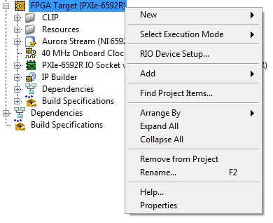
When you bring in your CLIP into the LV FPGA project, you must select the proper settings for your clocking and the lanes used on your High Speed Serial Instrument in order for LV FPGA to generate constraints behind the scene that is used for your design. One place is under the FPGA Target by right clicking and selecting Properties, then configuring the Component-Level IP for your project. This takes you to the Component-Level IP Wizard (CLIP Wizard) which will assist you in adding compilation critical files and also setting up internal constraints to be used during the LV FPGA compilation process: Using the Configure Component-Level IP Wizard (FPGA Module)
Figure 6: Right Click FPGA Target Reveals Properties Selection
The configuration of the IP through this wizard generates constraints based on the selections that you make during each step, so it is important to carefully consider all signals in your design which may need to be included in each step of the CLIP Wizard.
Another section of your LV FPGA project which will require modification is the High Speed Serial Instrument IO Socket, within the FPGA Target hierarchy. By right clicking and selecting Properties, you will be able to configure what CLIP declaration your project uses, as well as defining Clock Selections, Clocking and IO, Generic definitions, and Terminal data type:
Figure 7: Right Click IO Socket Reveals Properties Selection
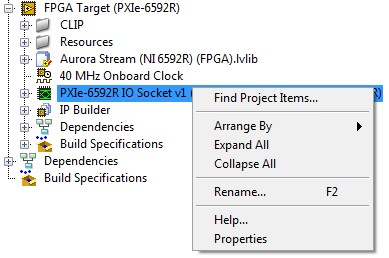
Figure 8: Clocking and IO Category Showing IO Configuration
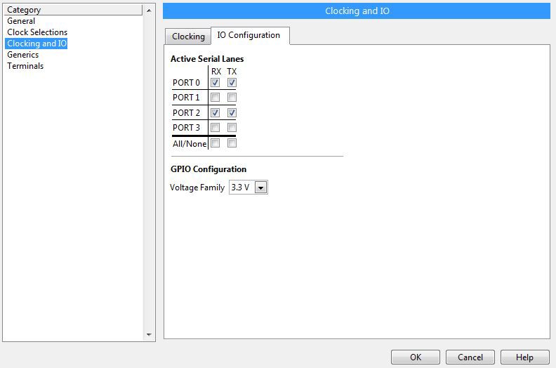
Important Note: you must visit the IO Configuration page at least once in your LV FPGA project before your first compilation. Here, you must select the exact lanes that your top level CLIP utilizes in order for the compilation to complete successfully.
Vivado Constraints Generator
Vivado offers a specific tool called the Constraints Generator which helps users create constraints for their design without having to have knowledge of the syntax which defines the constraint. For more information, please follow this link or go to Vivado Help: Xilinx Training Using the XDC Constraint Editor
Design Hierarchy in LV FPGA and the CLIP
When you add a Socketed CLIP definition into your LV FPGA project, generally you include your top level CLIP file, your user constraints, and any accompanying netlists which will be compiled into your final project. This is a brief overview of the design hierarchy and where those files fit into the overall design:
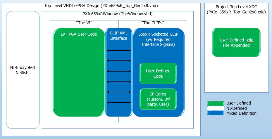
The hierarchy is important to understand when generating constraints since your constraints will reference paths in your design.
Important Info: The hierarchy of the constraints for a particular CLIP, which is compiled outside of the LV FPGA project in Vivado, will change when that CLIP is brought into LV FPGA at the top-most level. NI recommends using the %ClipInstancePath% token which contains the additional top level paths that are added in the LV FPGA project. Refer to the section Common Issues and Troubleshooting for more information.
Best Practices for Generating Constraints
As you build your constraints into your design, there are a few best practices that can be used to ensure the constraints are properly and efficiently designed for your application.
Organization
The organization of your constraints within the .xdc file helps the compiler correctly analyze the constraints in the design. The compiler will interpret constraints in a sequential manner, from top to bottom, until all constraints have been analyzed. The recommended constraint organization structure from Xilinx UG903 Using Constraints Guide is the following:
## Timing Assertions Section
# Primary clocks
# Virtual clocks
# Generated clocks
# Clock Groups
# Input and output delay constraints
## Timing Exceptions Section
# False Paths
# Max Delay / Min Delay
# Multicycle Paths
# Case Analysis
# Disable Timing
Naming
Be sure to include comments in your constraints file that clearly indicates the intent of the constraint, and the signal that is being acted upon. Clearly labeling this information, along with any decisions that went into including the constraint, will help any reader of the .xdc file to quickly identify the reason behind the constraint and its location in the design.
# User Clock Constraint: the value is selected based on the line rate of the module
create_clock -name TS_port0_user_clk_i -period 6.206 [get_pins %ClipInstancePath%/AuroraBlock.Port0_clock_module_i/user_clk_net_i/O]
Clocks
Be sure to create all clocks in your design, using create_clock, that are generated within the CLIP. An example of such clocks are TXOUTCLK and RXOUTCLK, which are generated by the GTXE2_CHANNEL primitive that resides in the CLIP of every MGT design. Any missing clock in your design could lead to issues where your compilation may pass timing, but fail to work consistently during functional testing.
If the clock is generated in the LV FPGA design, such as a base clock source from the LV FPGA project, you do not need to create constraints for these clocks. These constraints are automatically generated by your LV FPGA project.
Resets
Asynchronous resets which originate inside your CLIP should also be added to your constraints file in order to remove false timing violations that may occur. Identify all reset signals in your CLIP design and be sure to include constraints as required.
Info: If you choose to assign a top level reset signal in LV FPGA’s CLIP Wizard, you should not create a constraint for this signal in the .xdc file.
False Path and Max Delay
Some typical constraints that are used in your .xdc file are set_false_path and set_max_delay. Whether timing is evaluated on an asynchronous signal or a clock domain crossing, not including constraints for these paths will result in the tools incorrectly analyzing the timing for these paths, which could possibly result in timing failures. It is important to understand the implications and the correct application of set_false_path in order to successfully compile your design while not mistakenly ignoring time-critical paths in your design that need analysis.
Anytime set_false_path is used, care must be taken to understand where the constraint begins and where it ends. Using both –to and –from creates the most control over the path of interest to be ignored. Be careful using just one or the other, as connected paths other than the one you intend to constrain in the design may be ignored that are timing critical.
NI recommends only using set_max_delay constraints in place of set_false_path constraints. While both commands could be utilized to create a successfully constrained project, set_max_delay provides more timing control over path delay than set_false_path.
For instance, a path delay of 20 ns would not be reported to the designer if a set_false_path command was used, yet the compiler could choose to route your signal with any delay it needed based on the constraint. On the other hand, using set_max_delay at 10 ns would safely constrain the maximum path delay in the fabric to 10ns. Experiment with relaxing the maximum delay path value to find the optimal value for your particular design.
Clock Groups
When setting two clock domains asynchronous of each other in your constraints file, it is common to use the set_clock_groups Tcl command. This command will ignore any timing analysis between two clock domains. A scenario where using this command is acceptable is when you have a clock domain crossing between two clocks that exist entirely within the CLIP and are not related to one another.
With the High Speed Serial Instruments, there are multiple LV FPGA base clocks that are created and constrained for you in the design. Therefore, if any LV FPGA base clocks in the design need to be set asynchronous from a clock created in your CLIP, it is unsafe to use the set_clock_groups command. This is due to other parts of the design outside of the CLIP that may be affected by the clocking relationship. For instance, bringing a clock created in the CLIP into LV FPGA and setting it asynchronous of a base clock can create unsafe conditions where timing may need to be analyzed on the diagram and in the “black box” fixed logic of the LV FPGA design.
The best practice for constraining a properly implemented clock domain crossing is to clearly mark any clock domain crossings (CDCs) and their related D flop in the design, and use the set_max_delay or set_false_path command for all registers or FIFOs crossing into a new clock domain. Some example constraints that performs this function are below:
set_false_path -to [get_pins -hier *aurora_64b66b_cdc_to*/D] (all D inputs of cdc synchronization registers are ignored)
set_max_delay 10 -to [get_pins -hier *aurora_64b66b_cdc_to*/D] (all D inputs of cdc synchronization registers have maximum delay of 10 ns)
Creating .xdc Constraints
When you are creating a path to the pin or cell that you are trying to constrain, there are several different methods available to create the constraint path using Vivado constraint syntax. Here are some tips to consider while building the path to your pin, port, or cell in your design. A majority of this section is adopted from Xilinx UG903 Using Constraints Guide chapter 2, Creating Synthesis Constraints:
- When you first are creating your .xdc constraints, you may use the Tcl Console to validate the syntax of the .xdc commands before saving them in the .xdc files. This can be performed by creating a project in Vivado and opening the elaborated or synthesized design, which will then allow you to copy/paste constraints in the Tcl Console. Refer to the Xilinx UG903 guide for more information.
- It is recommended to avoid using -hierarchical in your constraints and explicitly use the / character at all levels of hierarchy to avoid potential problems with finding the path in memory. The reason is that Vivado synthesis can sometimes flatten hierarchy levels, which then removes some of the hierarchy path from memory. Creating a constraint that uses the -hierarchical option with partial paths, such as using wildcards across multiple levels of hierarchy, may return a warning that the object was not found. This example is adapted from the Xilinx UG903 guide:
RTL Design Example: register in overall design
inst_A/inst_B/control_reg
If the hierarchy is flattened, the following constraints will be found in the resulting flattened design. However, if the hierarchy is not flattened, they will not be found. Note that a wildcard is used to traverse multiple levels in both instances. Because a wildcard is used to represent multiple levels of hierarchy with the hierarchical command, Vivado cannot find the path in the design.
% get_cells –hierarchical *inst_B/control_reg (path not found/constraint not applied in design, missing inst_A level)
% get_cells inst_A*control_reg (path not found/constraint not applied in design, missing inst_b level)
Explicitly writing all or some part of every level in the hierarchy ensures that constraints are properly found in both flattened and unflattened hierarchies, leading up to the object you wish to constraint. The following is a correction to the above constraints to be found in any synthesis/implementation of control_reg. Wildcards are still used within a level of hierarchy, but do not traverse any hierarchy level:
% get_cells inst_A/inst_B/*_reg (successfully finds all pins/cells with *_reg at the control_reg level)
% get_cells inst_*/inst_B/control_reg (successfully finds all pins/cells with inst_* at the top inst_A level)
Please look at the following Xilinx Answer Record for more information: AR# 62136 Vivado Constraints - Understanding how hierarchy separator "/" works with wildcard * in XDC and UCF
- When working with NI Devices, we provide a %ClipInstancePath% token that appends the overall VHDL hierarchy used by the LV FPGA compiler to your existing top level VHDL path. For instance, if you have a constraint for your CLIP that works in Vivado, when you bring that constraint into LV FPGA, you may append the token to the beginning of the object path so that the compiler can still find it in memory:
% get_cells inst_A/inst_B/control_reg(Vivado constraint)
% get_cells %ClipInstancePath%/inst_A/inst_B/control_reg(LV FPGA constraint that adds additional hierarchy levels)
You may reference the Constraints and Hierarchy section of the NI High-Speed Serial Instruments User Manual for more information.
Design Analysis and Closure Techniques
When working with a VHDL design in Vivado, it is common to run into timing violations or design issues. Vivado has provided many tools for analysis and debug of a design as it relates to logic or constraints. One powerful tool that will help identify the need for timing constraints is the Report Timing Summary tool. You can use this tool once you have synthesized your design in Vivado. The report shows endpoints which are missing create_clock constraints (no_clock) or violate setup and hold timing (potential max_delay candidate). For more information on using various Vivado tools for analysis and timing closure, refer to the following link: Vivado Design Suite User Guide - Design Analysis and Closure Techniques
Common Issues and Troubleshooting
When creating constraints, you might find that you have some issues migrating constraints from the Vivado standalone environment into your LV FPGA project. The following items are common issues seen when porting Vivado designs into a LV FPGA project, and common troubleshooting techniques in order to help efficiently correct any issues that exist in the design.
Port vs Pin
When generating constraints for your NI High Speed Serial Instrument, you may have had some .xdc constraints from a previously working sample project that you are porting over into your LV FPGA project. In the LV FPGA project, your top level VHDL file (the CLIP) is actually a few levels below the High Speed Serial Instrument’s top level VHDL file within your LV FPGA project. It is common to see the following path appended to your top level VHDL file by using the %ClipInstancePath% token (where 659XR is replaced by the model number of your High Speed Serial Instrument):
PXIe659XRWindow/theCLIPs/PXIe_dash_659XR_IO_Socket_v1_CLIP0
This scenario creates an issue when referring to a “pin” vs a “port” in your top level VHDL. Since the port must be on the top level to be referenced, you will see warnings that the port does not exist when you bring your design into the LV FPGA project. To correct this, you must replace get_ports with get_pins in your .xdc constraints file, along with adding the %ClipInstancePath% token to the path. You also must replace the port name with the location of the clock output from the configured buffer in the fabric.
Example: the first constraint may work in Vivado stand alone, the second constraint is updated for porting to the LV FPGA project.
create_clock -name MgtRefClk0 -period 6.400 [get_ports MgtRefClk0]
create_clock -name MgtRefClk0 -period 6.400 [get_pins %ClipInstancePath%/AuroraBlock.MgtRefClk0IBuf/O]
Syntax Issues
Small mistakes in the naming of a path can generate a warning of:
“WARNING: [Vivado 12-584] No ports matched”
“WARNING: [Vivado 12-508] No pins matched”
“WARNING: [Vivado 12-180] No cells matched”
“WARNING: [Vivado 12-627] No clocks matched”
The best way to watch out for these warnings is to ensure the path you are searching for does exist in your design. Using Vivado, you can search the path in your synthesized design to see if it exists as it is written in your constraints file by using the Find tool.
Here are some common syntax issues that you may encounter in your constraints design:
- Missing brackets { } or [ ]
- The port or line number in a constraint is off:
- Port0_aurora_64b66b_i could be Port1 or Port2
- Wrong name of a signal
- RXOUTCLK vs RXOUTCLK0 vs RXOUT_CLK
Debugging the Timing Violation Analysis Window
As you work with LV FPGA Compilations, you may run into Timing Violations that show in the Compilation Status window. The help for the Timing Violation Analysis Window describes more about the features of the window.
In order to effectively debug these violations, it helps to understand the two main types of errors and their common reasons for failure. The first failure is an unrealistic timing requirement in your design:
Figure 9: Path Timing Requirement of 10 ps is Unrealistic for Design
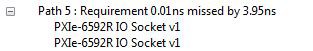
When you see this in the Timing Violation Analysis Window, this is your first step to resolve these violations in your design. Other violations may only be occurring due to the nature of the compiler trying to meet the unrealistic timing requirement. It will prioritize the tight path over other important timing critical paths, and having these requirements in your design will cause several points to fail all at once.
To resolve these tight timing violations, you must first understand the important of the path in your design. You can see the path by clicking on the items under the violation in the analysis window. The most common way to correct these issues is to issue a false path constraint so that the compiler no longer analyzes timing for this path.
There are typically other paths in the Timing Violation Analysis Window that you will see on any given compile:
Figure 10: Timing Violation Analysis Window
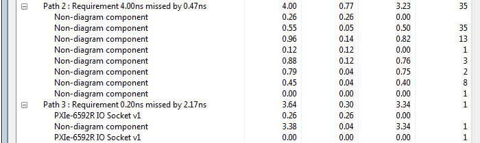
Requirements that look “normal”, in other words, they look like a period frequency to a real clock in your design, typically do not need correction when a Non-diagram component is the only items in the path. This is usually remedied once the unrealistic timing requirements are corrected. When there are paths in your LV FPGA diagram or your CLIP (PXIe-659xR IO Socket v1), and the requirement is reasonable (not unrealistic, some period interval of a clock you are using), you may have to use pipelining to ensure your logic can be performed within one clock cycle of the main clock driving the logic. Pipelining is explained more in depth for LV FPGA in the following help topic: Optimizing FPGA VIs Using Pipelining (FPGA Module)
Debugging Xilinx Log Files
When debugging Xilinx log files (lvXilinxLog.txt), there are some common practices which will help you efficiently identify and resolve problems that may arise in your design compilation:
- Search for Critical Warnings in your log file and resolve them
- User Constraints are analyzed after synthesis in the compilation flow: searching for the phrase “Processing XDC Constraints” in the lvXilinxlog.txt file should be where any warnings or critical warnings in the constraints are identified. As a user, it is your responsibility to take care of any warning/critical warnings directly related to user defined constraints.
- Warnings referencing constraints that you did not directly create should be ignored. The .xdc file you created is appended to a larger PXIe659XR_Top_Gen2x8.xdc file, which contains many automatically generated constraints. This is why you will see various warnings for constraints you did not produce. These constraints were generated by LV FPGA automatically, and do not have a negative impact on your design.
- If a user-defined constraint shows up as a warning/critical warning, then it is likely that the constraint was unapplied. Any user-defined constraints not indicated in this section of the log file were likely successfully applied.
- Most constraint warnings will give meaningful and helpful information next to that line, so be sure to read any hints as to why the warnings appeared.
Aurora IP Constraints Overview
As a helpful starting place to guide you towards creating your own constraints for a particular design, let us walk through one of our examples for the Aurora protocol on a PXIe-6592R High Speed Serial Instrument:
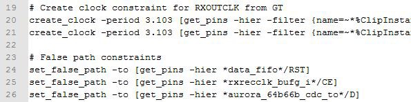
Figure 11: Example Project: Aurora 6592R Design Constraints
Let’s examine a few of the lines to see why these constraints were used, how they affect the design, and how to change them based on your own project:
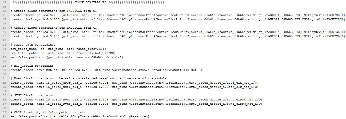
# Create clock constraint for TXOUTCLK from GT
create_clock -period 3.103 [get_pins -hier -filter {name=~*%ClipInstancePath%/AuroraBlock.Port0_aurora_64b66b_i*aurora_64b66b_multi_gt_i*AURORA_64B66B_GTX_INST/gtxe2_i/TXOUTCLK}]
create_clock -period 3.103 [get_pins -hier -filter {name=~*%ClipInstancePath%/AuroraBlock.Port2_aurora_64b66b_i*aurora_64b66b_multi_gt_i*AURORA_64B66B_GTX_INST/gtxe2_i/TXOUTCLK}]
# Create clock constraint for RXOUTCLK from GT
create_clock -period 3.103 [get_pins -hier -filter {name=~*%ClipInstancePath%/AuroraBlock.Port0_aurora_64b66b_i*aurora_64b66b_multi_gt_i*AURORA_64B66B_GTX_INST/gtxe2_i/RXOUTCLK}]
create_clock -period 3.103 [get_pins -hier -filter {name=~*%ClipInstancePath%/AuroraBlock.Port2_aurora_64b66b_i*aurora_64b66b_multi_gt_i*AURORA_64B66B_GTX_INST/gtxe2_i/RXOUTCLK}]
The TXOUTCLK and RXOUTCLK constraints are two vital clocks in many High Speed Serial designs. Both of these clocks are sourced within the CLIP, which is why they are created in the user defined constraints file. These declarations in the constraints file identify the frequency of the clocks and their location inside the design. If the clock speed changes in your design, you may simply change the period value to modify the constraint based on your project. Notice the use of the %ClipInstancePath% token.
The clocks are referenced by their pin, which is found by using the –filter attribute of the create_clock function. The syntax for these particular constraints were copied from Vivado after using the built in search tool to find the clocks within the elaborated design. Using Vivado’s built in search tool and resulting Tcl command is the recommended process to generate paths for your constraints and avoid path not found errors.
# False path constraints
set_false_path -to [get_pins -hier *data_fifo*/RST]
set_false_path -to [get_pins -hier *rxrecclk_bufg_i*/CE]
set_false_path -to [get_pins -hier *aurora_64b66b_cdc_to*/D]
The false path constraints set here basically identify asynchronous signals or clock domain crossings which should not be analyzed for timing. These are commonly copied over from an existing constraint file that is provided with the example IP. Since reset signals tend to be asynchronous, without constraints, your design will fail timing in a compilation because the required setup/hold time for that signal will always violate the synchronous requirement. Using set_false_path will tell the compiler to ignore timing on the identified signal path, thus preventing false timing failures.
For clock domain crossings (CDC), you must be careful to ensure your design has taken into account the CDC through a digital design method. For instance, using multi flop synchronizers or asynchronous FIFOs allow signals to safely pass from one clock domain to the next. Once this has occurred, you may tell the compiler to ignore the timing analysis on the signal path coming into the first flop of the synchronizer. A best practice for this is to name all signals going into a synchronizer/CDC circuit with “cdc_to” so that you can write one false path constraint for all cdc_to signals in your design. Many example designs from Xilinx use this methodology to identify CDC registers in the design.
References
Xilinx Training - Using the XDC Constraint Editor -
http://www.xilinx.com/training/vivado/using-the-xdc-constraint-editor.htm
Xilinx Vivado Design Suite User Guide - Using Constraints, UG903 (v2013.4) January 24, 2014 -
http://www.xilinx.com/support/documentation/sw_manuals/xilinx2013_4/ug903-vivado-using-constraints.pdf
Xilinx Vivado Design Suite User Guide - Using Constraints, UG903 (v2014.3,v2014.4) October 31, 2014 -
http://www.xilinx.com/support/documentation/sw_manuals/xilinx2014_4/ug903-vivado-using-constraints.pdf
Xilinx Training - Design Constraints Overview -
http://www.xilinx.com/training/vivado/design-constraints-overview.htm
Xilinx LogiCORE IP Aurora 64B/66B v9.2 - Product Guide, Vivado Design Suite, PG074 June 4, 2014 -
http://www.xilinx.com/support/documentation/ip_documentation/aurora_64b66b/v9_2/pg074-aurora-64b66b.pdf
Xilinx Vivado Design Suite User Guide - Design Analysis and Closure Techniques, UG906 (v 2012.3) November 16, 2012 -
http://www.xilinx.com/support/documentation/sw_manuals/xilinx2012_3/ug906-vivado-design-analysis.pdf