RIO Mezzanine Card Digital I/O Capabilities for Single-Board RIO
Contents
- Overview
- FPGA Sample Rate
- Signal Integrity
- RMC DIO Timing Specifications
- Asynchronous Example
- Synchronous Example
- Summary
- Additional Information
Overview
Certain Single-Board RIO controllers include a RIO Mezzanine Card (RMC) connector, which is a high-density, high-throughput connector that features 96 single-ended digital I/O (DIO) lines directly connected to the FPGA with the ability to add up to two C Series modules and more peripherals. Develop a custom RMC to integrate your own specific analog I/O, DIO, communication capabilities, and signal conditioning by combining these components onto a mating PCB. By controlling and monitoring the DIO lines with LabVIEW FPGA I/O nodes, you can rapidly implement your desired functionality in the FPGA. However, be careful when designing a custom RMC to ensure that you are meeting timing and signal integrity requirements.
NI has optimized the RMC connectivity on Single-Board RIO controllers for general-purpose use to offer a balance between ease of RMC implementation and signal performance. The FPGA I/O is connected to the RMC connector through a series termination resistor, and the FPGA drive and onboard signal termination support a wide range of applications. In general, this allows RMC implementations to exceed the performance levels (from a digital interface perspective) of an NI C Series module while retaining design flexibility options and robust signal integrity on the RMC.
This document provides Single-Board RIO platform timing parameters to use when analyzing the interface timing for a custom RMC. Note that the overall performance of the interface is not solely determined by the FPGA. Though you can compile the FPGA for relatively high clock rates (40 MHz, 80 MHz, 120 MHz, and so on), this does not mean that the entire signal chain can operate at those rates. Other factors (both on Single-Board RIO controllers and the RMC) such as signal loading, setup and hold times, skew, PCB routing, and more lower the effective signaling rate when implementing a particular protocol or interface. Refer to Table 1 for representative applications and typical frequencies that you can readily achieve using common design practices.
| Application | Typical Achievable Frequency |
| SPI | 10 MHz |
| Source Synchronous SPI | 20 MHz |
| Asynchronous Output | 60 MHz |
| Asynchronous Input | 60 MHz |
Table 1: Typical Operating Frequencies
This table should not be treated as a guaranteed upper limit. Some applications (due to the implementation of the circuitry on the RMC) may run considerably slower (such as an SPI protocol implemented through slow optoisolators). Other applications (through careful optimization and analysis) may be able to run notably faster.
Customers with significantly higher performance requirements should contact NI.
FPGA Sample Rate
The DIO sample frequency is directly related to the loop rate used in LabVIEW FPGA. An example single-cycle Timed Loop is shown in Figure 1.
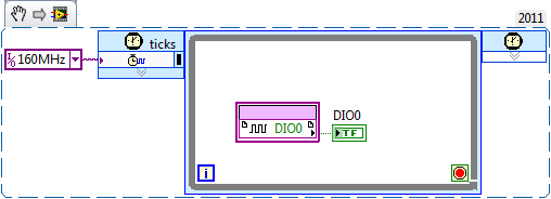
Figure 1: Single-Cycle Timed Loop Using 160 MHz Derived Clock
This loop, timed by a 160 MHz derived clock, is reading a single DIO channel. As long as this successfully compiles, the FPGA is sampling that DIO at 160 MHz. In the case of non-single-cycle loops, the DIO is sampled at that structure's loop rate. However, just because a VI compiles successfully does not mean that the overall system (Single-Board RIO, RMC, and external devices) is going to function correctly. Some indirect limitations to the DIO’s maximum frequency include signal integrity and timing requirements. These limitations vary from one application to the next.
Signal Integrity
FPGA drive characteristics, termination resistors, and PCB layout all affect signal integrity on a Single-Board RIO controller. To be as forgiving as possible for RMC layouts, these attributes have been tuned to support a wide range of trace lengths and digital loads. However, you still need to consider some features of the RMC layout to ensure the best possible signal integrity.
Route RMC DIO signals with 55 Ω characteristic trace impedance.
The DIO lines through the RMC connector have a 55 Ω trace impedance, and designing RMCs the same way reduces impedance mismatches and, in turn, reduces unwanted reflections along the signal path. Trace impedance is the result of both PCB and trace geometry (dialectic thickness, trace width and spacing, and so on). Since the PCB geometry affects the trace impedance, it is best to work with the PCB manufacturer to provide the required trace geometry for its manufacturing process.
Evaluate signal integrity on the RMC for all applications.
Ideally, signals at their destinations have smooth monotonic edges with no overshoot. For a 50 percent duty-cycle clock, a general rule of thumb is to be high at least one-third of the period and low at least one-third of the period. This leaves at most another one-third of the period to spend in transition. Table 1 shows that an asynchronous output’s typically achievable frequency is 60 MHz. This is based on the clock rule of thumb with a 10 pF load at the RMC connector. The asynchronous input specified in Table 1 is also based on this rule but with an LVC driver and 49.9 Ω series termination.
Provide properly tuned series termination as close to the driver's pin as possible for digital inputs.
The Single-Board RIO controller uses 33 Ω series termination at the FPGA. For edge rates less than 10 ns, series termination is strongly recommended.
Follow digital design best practices.
Following digital design best practices is always a good idea and has a positive impact on signal integrity. Some things to keep in mind when designing an RMC include minimizing layer changes and vias, maintaining a continuous reference plane, connecting lines to single loads, and properly decoupling digital ICs.
RMC DIO Timing Specifications
Many applications have timing requirements that you need to evaluate. Table 2 contains the RMC DIO specifications necessary to validate timing. The following specifications at the RMC connector are valid across the Single-Board RIO controller's operating temperature range.
| Symbol | Parameter | Conditions | Min | Max | Unit |
| tSU | DIO Setup | 6 | - | ns | |
| tHO | DIO Hold | 4 | - | ns | |
| tCO | FPGA Sample Clock to DIO Out | CLOAD = 20 pF | - | 19 | ns |
| CLOAD = 50 pF | - | 22 | ns | ||
| tSKEW | DIO to DIO Skew | CLOAD = 20 pF | - | 12 | ns |
| CLOAD = 50 pF | - | 15 | ns | ||
| CINPUT | DIO Input Capacitance | - | 30 | pF |
Table 2: DIO Timing Specifications at the RMC Connector
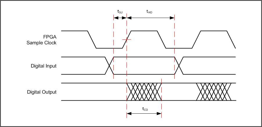
Figure 2: DIO Timing Diagram at the RMC Connector
FPGA Sample Clock
For the purposes of discussing timing in this document, the FPGA sample clock is the internal FPGA clock that is registering the DIO channel. This clock is based on the 40 MHz onboard clock. When using DIO inside a single-cycle Timed Loop, the FPGA sample clock is the clock timing the loop. Outside single-cycle Timed Loops, the FPGA sample clock is the target’s top-level clock.
DIO Setup
DIO Setup is the minimum time a DIO signal must be stable at the RMC connector before the FPGA sample clock’s edge to guarantee the current value is latched on that edge.
DIO Hold
DIO Hold is the minimum time a DIO signal must be stable at the RMC connector after the FPGA sample clock’s edge to guarantee the current value is latched on that edge.
FPGA Sample Clock to DIO Out
FPGA Sample Clock to DIO Out is the maximum time that it takes a DIO line to change state at the RMC connector after the FPGA sample clock’s edge. This specification is valid only if synchronizing registers are used in the I/O Node. These are turned on by default.
The FPGA Sample Clock to DIO Out varies based on the capacitive load on the RMC. The 20 pF and 50 pF values have been given. When you calculate this load, include the trace, vias, and package pins in the calculation. A point-to-point connection between a DIO channel and a single digital input is generally less than or equal to 20 pF. Many devices have input capacitance specifications in their data sheets. A rule of thumb for trace capacitance of a 55 Ω transmission line is 3.8 pF per inch. This varies based on PCB geometry.
To guarantee accurate timing calculations, always use the next highest capacitance value. For example, if the load is 25 pF, you should use the 50 pF tCO.
DIO to DIO Skew
DIO to DIO Skew is the maximum skew between all DIO channels. This specification accounts for both the maximum board skew on the Single-Board RIO controller and the maximum skew inside the FPGA. It is valid only when synchronizing registers are used in the I/O Node. These are turned on by default.
The skew varies based on the capacitive load on the RMC. The 20 pF and 50 pF values have been given. When calculating this load, you should include the trace, vias, and package pins in the calculation. Many devices have input capacitance specifications in their data sheets. A rule of thumb for trace capacitance of a 55 Ω transmission line is 3.8 pF per inch. This varies based on PCB geometry.
For skew between channels with different loads, you should use the higher load’s skew. For example, if an SPI CLK’s load is 10 pF and the Master Out Slave In (MOSI) load is 30 pF, you should use the 50 pF tSKEW for timing calculations involving these two signals.
DIO Input Capacitance
DIO Input Capacitance is the maximum input capacitance at the DIO connector. This specification includes the input capacitance of the FPGA and the capacitance of the trace, vias, and RMC connector on the Single-Board RIO controller.
Asynchronous Example
Asynchronous use cases have no external timing requirements. However, timing specifications along with FPGA sample rate and signal integrity still limit the frequency. Figure 3 shows an example of implementing a simple counter/timer.
Counter/Timer
When implementing a counter in LabVIEW FPGA, the external signal and the FPGA sample clock have no guaranteed timing relationship. They must be treated as completely asynchronous to each other. To make sure that every edge of the external signal is registered, the FPGA sample clock must be greater than 2X faster than the external signal. How much greater depends on the frequency of the external signal and the Single-Board RIO controller's setup and hold specifications.
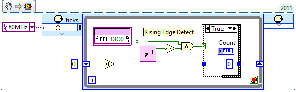
Figure 3: Example Counter
Figure 3 shows a simple VI that counts the number of loop iterations between rising edges on DIO0. Notice that the loop is timed using an 80 MHz derived clock and is registering DIO0 at this rate. Intuitively, it may seem that the Nyquist theorem applies and this example can accurately detect 40 MHz signals. This is not the case, however, due to the setup and hold requirements.
Figure 4 shows how an external signal’s phase could line up so that it always violates the setup and hold requirements. When a signal transitions inside the setup/hold window, any value can be registered by the FPGA. In Figure 4, every transition is inside the setup/hold window. The counter's behavior is unpredictable.
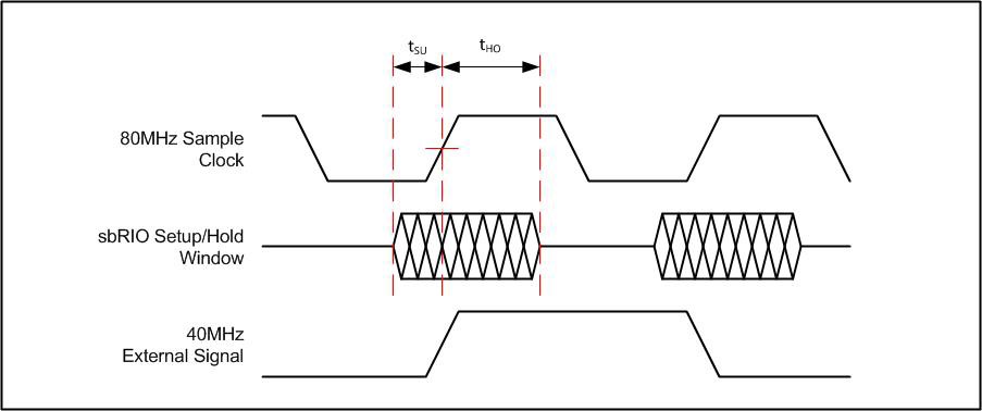
Figure 4: Failing Counter Timing
The external signal and the sample clock are asynchronous and have no guaranteed phase relationship. Sometimes the external signal is going to transition inside the sample clock's setup/hold window. This is fine as long as the external signal does not transition again before the next setup/hold window has passed. In this scenario, if the external signal’s transition is not detected on the first sample clock edge, it is detected on the second.
For a counter to detect every edge of the external signal, the external signal's pulse width must be greater than the sample clock period plus setup and hold times. For this example, the timing works out as follows.
80 MHz Sample Clock Period = 12.5 ns
Minimum External Signal Pulse Width = Sample Clock Period + tSU + tHO
Minimum External Signal Pulse Width = 12.5 ns + 6 ns + 4 ns
Minimum External Signal Pulse Width = 22.5 ns
Maximum External Signal Frequency = 22.22 MHz
Note: This is the maximum external frequency at which every edge is guaranteed to be detected with an 80 MHz sample rate across temperature and part tolerances. This number is based on the Single-Board RIO controller's worst-case ratings. Real-world testing with any given Single-Board RIO controller typically shows much higher frequencies working correctly. These results, however, cannot be guaranteed with all Single-Board RIO controllers across the operating temperature range.
Note: Faster sample rates provide more granularity in the counter's results regardless of the external signal's frequency.
Synchronous Example
SPI Timing
The following is an example of how to verify timing on the RMC connector with an SPI interface. SPI is a very common and versatile protocol, and this example assumes a working knowledge of SPI protocol requirements.
This example calculates the timing margin with a 10 MHz SPI CLK. If there is a positive margin for each constraint, then timing is successfully being met. For any SPI application, the easiest solution to a negative margin is to slow down the SPI CLK.
The Single-Board RIO controller is acting as the SPI master, and the SPI slave for this example is an SPI EEPROM. The data lines are updated on the falling edge of the SPI CLK and registered at the other device on the rising edge. You need the EEPROM’s timing specifications to verify timing, and example specifications are shown in Table 3. For a different SPI slave device, you need to obtain the information in Table 3 from that device's data sheet.
| Symbol | Parameter | Conditions | Min | Max | Unit |
| slaveSU | MOSI Setup | 10 | - | ns | |
| slaveHO | MOSI Hold | 10 | - | ns | |
| slaveCO | MISO Clock to Out | CLOAD = 100pF | - | 20 | ns |
Table 3: Example EEPROM SPI Timing Specifications
SPI devices also have timing requirements related to the slave select line. These are generally not the limiting factor in SPI performance; however, you should account for them in an actual design. Timing analysis for slave select is similar to MOSI.
MOSI Setup
The slave device’s setup is the minimum amount of time MOSI must be stable before the latching edge of SPI CLK to guarantee the current value is registered.
MOSI Hold
The slave device’s hold is the minimum amount of time MOSI must be stable after the latching edge of SPI CLK to guarantee the current value is registered.
MISO Clock to Out
Master In Slave Out (MISO) Clock to Out is the maximum time it takes the slave device to drive MISO after it has received the falling edge of SPI CLK. It is typically specified with a capacitive load. In this example, the load is 100 pF. This means the specification is valid as long as the load on MISO is less than or equal to 100 pF.
MOSI Timing
For calculating the MOSI setup margin, the maximum margin is half of the SPI CLK's period. This is because MOSI is updated on the one edge of SPI CLK and latched on the other. The Single-Board RIO controller's maximum skew must be subtracted from the margin because both MOSI and SPI CLK are DIO channels. The slave device's setup also reduces the margin. Finally, any skew between the SPI CLK and MOSI on the RMC should be removed from the margin. A skew of 1 ns is conservative for a well-designed RMC with point-to-point signal routing and trace length matching to 1 in.
MOSI Setup Margin = SPI_CLK_Period/2 – tSKEW – slaveSU – RMCSKEW
MOSI Setup Margin = 50 ns – 12 ns – 10 ns – 1 ns
MOSI Setup Margin = 27 ns
The calculation for the MOSI hold margin is similar to setup except the slave device's hold specification is used instead of its setup specification. Skew is still included since the skew may occur in either direction. Depending on the direction of the skew, it reduces either the setup or hold timing margin, but it should be included in both as a worst case.
MOSI Hold Margin = SPI_CLK_Period/2 – tSKEW – slaveHO – RMCSKEW
MOSI Hold Margin = 50 ns – 12 ns – 10 ns – 1 ns
MOSI Hold Margin = 27 ns
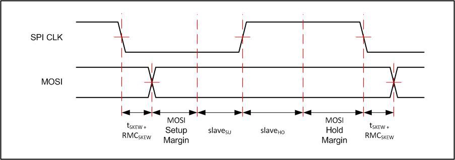
Figure 5: MOSI Timing at Slave Device
MISO Timing
MISO setup margin is a round-trip calculation. It must include the time it takes the SPI_CLK to reach the slave device and the time it takes MISO to reach the RMC connector. tCO is the maximum time it takes the falling edge of SPI_CLK to arrive on the RMC connector. RMCSCLK_PROP_DELAY is the propagation delay on the RMC from the connector to the slave device. Next, the slave device's clock to out must be removed from the margin. Then, the propagation delay of MOSI from the slave device back to the RMC connector is subtracted. Finally, the setup time of the RMC connector must be met and therefore removed from the margin.
For the RMC propagation delays, 1 ns is used in this example. This number varies based on the design of the RMC. 1 ns is a conservative number for RMCs designed with 55 Ω trace impedance and trace lengths less than 4 in. Propagation delays for the Single-Board RIO controllers have already been accounted for in the RMC timing specifications.
MISO Setup Margin = SPI_CLK_Period/2 – tCO – RMCSCLK_PROP_DELAY – slaveCO – RMCMISO_PROP_DELAY – tSU
MISO Setup Margin = 50 ns – 19 ns – 1 ns – 20 ns – 1 ns – 6 ns
MISO Setup Margin = 3 ns
The MISO hold calculation is similar to the MOSI hold. This is because the worst case for hold removes many of the setup variables. Propagation delays help hold margin, so as a worst case they are assumed to be zero. The slave device's clock to out also increases hold margin, so it too is assumed to be zero. That leaves any skew between the SPI CLK and MISO signals that could reduce hold margin and the RMC connector's minimum hold time.
MISO Hold Margin = SPI_CLK_Period/2 – tSKEW – RMCSKEW – tHO
MISO Hold Margin = 50 ns – 12 ns – 1 ns – 4 ns
MISO Hold Margin = 33 ns
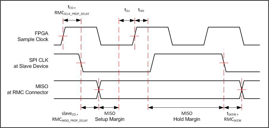
Figure 6: MISO Timing
Note: For any other synchronous interfaces, you should conduct similar calculations to ensure timing is met.
Summary
For any application, the FPGA sample rate, signal integrity, and timing requirements all contribute to the application's maximum frequency. The FPGA sample rate is constrained by successful compilation in LabVIEW FPGA. A well-designed RMC is required to ensure that signal integrity has a minimal impact on performance. Finally, both the Single-Board RIO and RMC devices' timing requirements have to be met to ensure successful operation. For each application, you should evaluate all of these factors to determine its maximum performance.