How-to: Using SPI and FPGA with LabVIEW and Embedded Sensors
Overview
This document describes the steps and structure utilized when creating sensor drivers using SPI. To use this document, you should have a basic understanding of embedded sensors and be familiar with the operation of LabVIEW. Furthermore, the users must have an understanding of the SPI communication protocol.
Contents
What are Embedded Sensor Drivers?
Sensor drivers are a set of VIs which allows the user to interact with an embedded sensor. Each VIs corresponds to a specific operation, such as configuring, reading, writing. Sensor drivers allow users to develop applications which interact with said sensors without the need to understand the communication and programming protocol. Furthermore, sensor drivers will save the developer development time and cost. Well documented sensor drivers are flexible and end users can customize the operations for their needs.
Example sensor drivers are already available for a variety of embedded sensors such as:
- ADIS16003 Dual-Axis Accelerometer
- ADIS16060 Digital Gyroscope
- ADIS16250 Low Power Gyroscope
- ADIS16350 Triple Axis Gyro & Accelerometer
- ADIS16209 Inclinometer
In this document we will outline the main steps in creating sensor drivers. Furthermore, as a practice exercise, we will develop the drivers for the ADIS16250 Low Power Gyroscope. The datasheet of this sensor can be found here.
LabVIEW Sensor Drivers Model
A sensor driver consists of the API VIs the user calls from a higher level application. The figure bellow illustrates how the instrument drivers interact with the application.
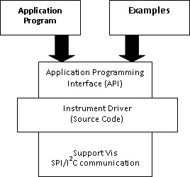
The Internal structure of the Sensor driver define the organization of the sensor drivers VIs. All user-accessible API VIs are organized into a modular hierarchy based on instrument functionality.
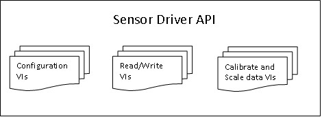
Configuration VIs
These VIs are used to configure the communication protocol with the sensor. In the case of the ADIS16250 the communication protocol is SPI (serial peripheral Interface). The configuration VIs will often define the speed at which to communication with the sensor as well as selecting the mode of operation. In the case of the ADIS16250 we need to set the Clock Rate (Hz), the clock polarity (CPOL), the clock phase (CPHA) and the Chip select (CS). In the Timing specifications of the sensor’s datasheet we can see that fsclk must be between the ranges of 10,000 Hz to 2,500,000 Hz. Furthermore, according to the timing diagram (figure 3) Chip select (CS) must be set to 0. Furthermore, clock phase and clock polarity must both be 1 for SPI communication
.
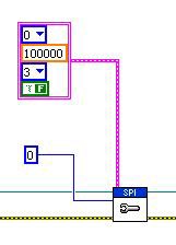
Figure 1. Setting up configuration parameter for ADIS16250
Read/Write VIs
These VIs are used to read or write from or to the sensor. Most SPI sensor will work in full duplex mode, that is to say every time it writes a bit it will read a bit as well. Thus when reading value from the sensor, the data will only be returned on the subsequent read/write command. In other words, the first read/write command will indicate to the sensor which value you which to read, the second read/write command will return the data from the sensor.
Most sensors implement a simple register structure. This means all output and user-programmable functions are stored in registers with specific address. In the case of the ADI16250 Gyroscope, each register is defined with two 6 bit addresses for the upper and lower half of the register. To perform an operation we must first specify whether we which to read or write, then we must specify the address of either the output or user-programmable function we which to access, finally for a write command we must specify what to write. The figure below graphically demonstrates how to read or write a command the ADIS16250 sensor.
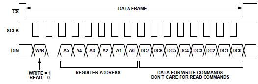
Figure 2: Bit sequence
In Figure 2, DIN line represents 16 bits of data which will be sent by SPI to the sensor. The first bit will either be a 1 or 0 to write or read respectively. The second bit will always be low. Bits A5 to A0 represent the address of the outputs or user-programmable function you wish to access, the address may consist of the lower or upper address of that register. Bits DC7 to DC0 contains the data which need to be written during a write command. During a read command the last 8 bits aren’t used. This timing bit sequence is typical of many SPI sensors; however you must consult the sensor specific datasheet to confirm this.
The address of the outputs of user-programmable register can be found on the datasheet. In the case of the ADIS16250, the register which contains the gyroscope data has addresses 0x05 and 0x04. Following the communication protocol above, if we wish to read data from the gyroscope we would perform a read/write command and write binary 0000010100000000. Starting from left to right, the first 0 indicates a read operation, the second bit is always low and the next six bits (000101) indicate the address of the register you wish to read. The last 8 bits are 0 in this case, since we are performing a read operation. During a write operation the last 8 bits will contain the data you wish to write.
Calibrate and Scale data VIs
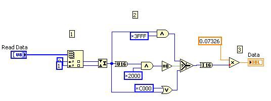
These VIs are used to convert the raw,un-scaled binary output data from the sensor into meaningful numeric data for our application. Converting and scaling binary data into numeric data will vary for any given sensor. You must consult the sensor datasheet to see how the output data is formatted. In the case ADIS16250 we are told that the sensor outputs 16 bits.
ND | EA | D13 | D12 | D11 | D10 | D9 | D8 | D7 | D6 | D5 | D4 | D3 | D2 | D1 | D0 |
ND bit is used to indicate if the data is new. The EA bit is used to indicate whether there was system error. The other 14 bits are the data. In the case of the gyroscope, these 14 bits are formatted two's complement with a scale factor of 0.07326o/sec/LSB. To convert the binary data into numeric data we must apply two's complement to the 14 bit output and multiply it by the LSB scale factor to obtain the degrees/sec value. LabVIEW automatically performs two's complement when converting from an unsigned 16 bit number to a 16 bit integer. Knowing this, the only step we must perform is sign extend the 14 bit output to 16 bits. Sign extending is the operation of padding a binary number on the left with either 1 or 0 depending on if the MSB of the original binary value is either 1 or 0 respectively.
14 bit binary value | Sign extended 16 bit value |
11110111011110 | 1111110111011110 |
00110111011110 | 0000110111011110 |
Once the sign extend has been completely we can simply convert the value to a 16 bit integer.
Once we are finished converting and scaling the value we can then manipulate the data however we choose using filters or other mathematical functions.
Important C
Documenting Vis
Document the VIs you create so information appears in the LabVIEW Context Help window for each sensor driver.
Conclusion
Designing modular and well documented sensor drivers will allow end-users to efficiently interact with the sensors without the need to understand the communication protocol and implementation protocol of the sensor.