Tutorial: Creating Test Benches
- Updated2026-03-17
- 8 minute(s) read
The tutorial in this topic covers the steps to complete to create a test bench for a simple FPGA VI that inverts values. Although the logic in the test bench will differ based on the logic in the FPGA VI you are testing, this tutorial outlines the common steps. The tutorial assumes knowledge of creating VIs.
Creating an FPGA VI to Test
Complete the following steps to create an FPGA VI to test in this tutorial.
- Create a LabVIEW project and save the project as inverter.lvproj.
- Add an FPGA target to the project.
- Right-click the FPGA target and select New»VI from the shortcut menu to create a new FPGA VI.
- Save the FPGA VI as Inverter.vi.
- Create two digital FPGA I/O items called input and output, respectively.
- Drag the FPGA I/O items from the Project Explorer window to the block diagram of the Inverter VI to create corresponding FPGA I/O Nodes.
- Right-click output on the FPGA I/O Node and select Change to Write from the shortcut menu.
- Place the FPGA I/O Nodes within a While loop and wire the nodes together, as
shown in the following block diagram:

The purpose of the Inverter VI is to read a digital line, invert the value, and write the inverted value to another digital line. Notice that the block diagram contains an error. The block diagram is missing a Not function between the two FPGA I/O Nodes.
Testing the FPGA VI on the Development Computer with Random Data
Complete the following steps to test the logic of the FPGA VI using random data for the input.
- Right-click the FPGA target and select Properties from the shortcut menu.
- In the FPGA Target Properties dialog box, select Execution Mode from the Category list to display the Execution Mode page.
- In the Simulation pull-down menu, select Use Simulated I/O.
- Click the OK button.
- On the block diagram of the FPGA VI, right-click the wire connecting the two FPGA I/O Nodes and select Probe from the shortcut menu to create a probe.
- Run the FPGA VI. Notice that the probe indicates values of TRUE and FALSE randomly.
- Stop the FPGA VI.
Testing the FPGA VI on the Development Computer with a Custom VI
Complete the following steps to test the FPGA VI using a custom VI test bench.
- On the Execution Mode page of the FPGA Target Properties dialog box, select Use Custom VI for FPGA I/O from the Simulation pull-down menu.
- Click the New VI from Template button and save the custom VI as Simulated IO for Inverter.vi.
- Click the Add button in the dialog that asks if you want to add the VI to the current project. Notice that LabVIEW adds the custom VI under My Computer in the project.
- Open the block diagram of the Simulated IO for Inverter VI, read the comments in
the VI, and delete the comments to reduce clutter on the block diagram. The
block diagram of the Simulated IO for Inverter VI appears as shown in the
following illustration:

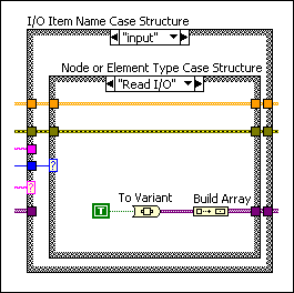
- Right-click the I/O Item Name Case structure and select Duplicate Case from the shortcut menu.
- Enter input in the selector label. The
input case executes when the FPGA VI calls the FPGA
I/O Node for the input I/O item. Note If you are using CLIP to pass data to the FPGA VI, you must place an extra backslash in the selector label for name of the CLIP I/O. For example, if the CLIP I/O item is CLIP\Port A, you must enter CLIP\\Port A in the selector label. The first backslash acts as an escape character for the second backslash in the name.
- Right-click the Node or Element Type Case structure and select Duplicate Case from the shortcut menu. Notice that the Read I/O case is selected. This case executes for the FPGA I/O Node configured to read the input I/O item.
- Delete the Report Support Error VI from the case and wire sim I/O info in and error out through the Case structure.
- Replace the empty array with a True constant, To Variant function, and Build
Array function as shown in the following block diagram:
- Run the Inverter VI. Notice that the probe on the wire between the two FPGA I/O Nodes indicates a value of TRUE because you included a True constant in the Simulated IO for Inverter VI. LabVIEW also returns an error message indicating that you did not specify behavior for the FPGA I/O Node configured for the output I/O item.
Testing the Output I/O Item
- In the Project Explorer window, select My Computer and then select File»New to display the New dialog box.
- Select Global Variable from the Other Files folder to create a new global VI.
- Save the global VI as Test Bookkeeping.
- Add a Boolean indicator called failed to the front panel of the Test Bookkeeping VI. The failed indicator is a global variable.
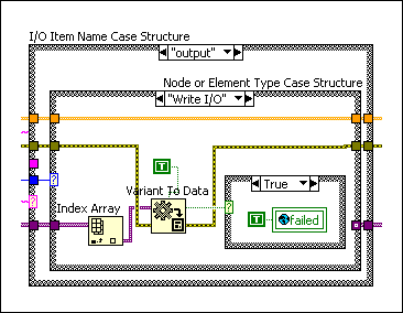
- On the block diagram of the Simulated IO for Inverter VI, right-click the input case of the IO Item Name Case structure and select Duplicate Case from the shortcut menu. Name the case as output.
- In the Node or Element Type Case structure, select the Read I/O case, double-click the selector, and enter Write I/O. This case executes for the FPGA I/O Node for the output I/O item.
- Delete the code that goes to the array of variants tunnel and add the Index
Array function, Variant To Data function, and a Case structure with the
failed global variable, as shown in the following
block diagram. Because you specified TRUE as the value for the
input I/O item, the value the Inverter VI writes to
the output I/O item should be FALSE, if the code in the
Inverter VI is correct. So, the test fails if the Inverter VI ever writes TRUE
to the output I/O item.
- Run the Inverter VI and monitor the Test Bookkeeping VI. Notice that the failed indicator is TRUE, indicating that the test failed.
- Stop the Inverter VI.
- To fix the problem in the Inverter VI, add a Not function as shown in the
following block diagram:

- In the Test Bookkeeping VI, right-click the failed indicator and select Data Operations»Reinitialize to Default Value from the shortcut menu. Now, when you run the Inverter VI, notice that the failed indicator remains FALSE, indicating that the test is not failing.
Testing the FPGA VI with a More Complex Custom VI
Complete the following steps to test that the Inverter VI behaves correctly for 10 selected input values supplied sequentially.
- In the Project Explorer window, right-click My Computer and select New»VI from the shortcut menu.
- Save the VI as Test Stimulus.vi.
- Update the Test Stimulus VI as shown in the following block diagram:

- Build the connector pane of the Test Stimulus VI so that you can use the VI as a subVI later in this tutorial.
- In the Test Bookkeeping VI, add a stimulus index control
that is a 32-bit signed integer. Also, add a test
complete Boolean indicator, as shown in the following front
panel:

- In the Simulated IO for Inverter VI, update the
Initializing case of the Execution
Stage Case structure to initialize the values from the Test
Bookkeeping VI as shown in the following block diagram. LabVIEW creates a clone
of the custom VI for each case in the Execution Stage
Case structure. If you want to share data between different cases, you can use
globals, as shown in the following block diagram, or some other mechanism that
accounts for the cloned cases, such as non-reentrant subVIs.

- Select the Running case from the Execution Stage Case structure, the input case from the I/O Item Name Case structure, and the Read I/O case from the Node or Element Type Case structure.
- Update the code for the Read I/O case of the
Node or Element Type Case structure as shown in the
following block diagram:

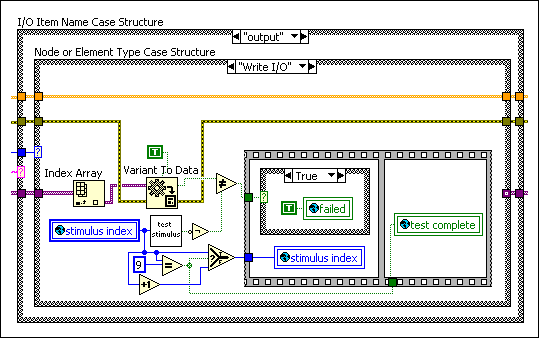
- Select the output case from the I/O Item Name Case structure and the Write I/O case from the Node or Element Type Case structure.
- Update the code for the Write I/O case of the
Node or Element Type Case structure as shown in the
following block diagram. The block diagram below gets the same stimulus as the
read for the input, inverts the stimulus, compares the stimulus to the value the
FPGA I/O Node receives, and declares test failure if the values are different.
The block diagram also increments stimulus index until
the index reaches 9, at which point the block diagram sets the test
complete global variable to TRUE.
- Run the Inverter VI and monitor the global variables in the Test Bookkeeping VI. Notice that stimulus index increases to 9, failed remains FALSE, and test complete remains FALSE until stimulus index reaches 9.
- Stop the Inverter VI.
Using a Host VI to Automate Execution of the Test Bench
The test bench you created above requires some manual work to run an interpret results. To simplify repetition of the test, complete the following steps to create a host VI to automate execution of the test bench.
- In the Project Explorer window, right-click My Computer and select New»VI from the shortcut menu.
- Save the VI as Test Controller.vi and update the VI as shown in
the following block diagram:

The Test Controller VI opens a reference to the Inverter VI and monitors the execution of the Inverter VI through global variables. After the test is complete or an error occurs, writing TRUE to the stop control stops the Test Controller VI. The Invoke Method configured for the Get FPGA VI Execution Mode method does not impact the execution, but the Invoke Method does provide access to any errors that might occur during execution of the FPGA VI on the development computer.