Digital Signal Processing FPGA VIs
- Updated2025-11-22
- 88 minute(s) read
Digital Signal Processing FPGA VIs
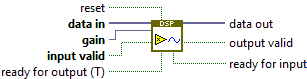
Digital Gain - Real - 1 spc.vi
Digitally controls the data in signal levels. This VI must be used in a single-cycle Timed Loop.
This VI provides the following functionality:
data out <= data in * gain
Where "*" represents scalar multiplication.
Data Type
This VI automatically adapts to real or complex data in types. It also automatically adapts to the data in array size. Arrays represent parallel samples from one data stream. For array sizes greater than one, the first element ('data in'[0]) is the oldest sample in the array.
Overflows
Overflows on data in.overflow are pipelined along with the data path, combined with overflows that occur inside of this VI, and output on data out.overflow.
Reset
Toggle the reset input to TRUE and then FALSE to reset the internal state of this VI. While in reset, ready for input and output valid are FALSE and input valid is ignored. This VI starts a reset operation when the reset input is set to TRUE or when the LabVIEW FPGA reset method is called.
Pipeline Delay
3 single-cycle Timed Loop clock cycles
Approximate resource usage in a Xilinx Kintex 7
Slice flip-flops: 50
Slice LUTs:: 80
Block RAMs (18kb): 0
DSP48E(1)s: 1
Approximate maximum single-cycle Timed Loop clock rate in a Xilinx Kintex 7
160 MHz

Digital Gain - Real - 2 spc.vi
Digitally controls the data in signal levels. This VI must be used in a single-cycle Timed Loop.
This VI provides the following functionality:
data out <= data in * gain
Where "*" represents scalar multiplication.
Data Type
This VI automatically adapts to real or complex data in types. It also automatically adapts to the data in array size. Arrays represent parallel samples from one data stream. For array sizes greater than one, the first element ('data in'[0]) is the oldest sample in the array.
Overflows
Overflows on data in.overflow are pipelined along with the data path, combined with overflows that occur inside of this VI, and output on data out.overflow.
Reset
Toggle the reset input to TRUE and then FALSE to reset the internal state of this VI. While in reset, ready for input and output valid are FALSE and input valid is ignored. This VI starts a reset operation when the reset input is set to TRUE or when the LabVIEW FPGA reset method is called.
Pipeline Delay
4 single-cycle Timed Loop clock cycles
Approximate resource usage in a Xilinx Kintex 7
Slice flip-flops: 130
Slice LUTs:: 170
Block RAMs (18kb): 0
DSP48E(1)s: 2
Approximate maximum single-cycle Timed Loop clock rate in a Xilinx Kintex 7
160 MHz
Digital Gain - Real - 4 spc.vi
Digitally controls the data in signal levels. This VI must be used in a single-cycle Timed Loop.
This VI provides the following functionality:
data out <= data in * gain
Where "*" represents scalar multiplication.
Data Type
This VI automatically adapts to real or complex data in types. It also automatically adapts to the data in array size. Arrays represent parallel samples from one data stream. For array sizes greater than one, the first element ('data in'[0]) is the oldest sample in the array.
Overflows
Overflows on data in.overflow are pipelined along with the data path, combined with overflows that occur inside of this VI, and output on data out.overflow.
Reset
Toggle the reset input to TRUE and then FALSE to reset the internal state of this VI. While in reset, ready for input and output valid are FALSE and input valid is ignored. This VI starts a reset operation when the reset input is set to TRUE or when the LabVIEW FPGA reset method is called.
Pipeline Delay
4 single-cycle Timed Loop clock cycles
Approximate resource usage in a Xilinx Kintex 7
Slice flip-flops: 260
Slice LUTs:: 320
Block RAMs (18kb): 0
DSP48E(1)s: 4
Approximate maximum single-cycle Timed Loop clock rate in a Xilinx Kintex 7
160 MHz

Digital Gain - Real - 8 spc.vi
Digitally controls the data in signal levels. This VI must be used in a single-cycle Timed Loop.
This VI provides the following functionality:
data out <= data in * gain
Where "*" represents scalar multiplication.
Data Type
This VI automatically adapts to real or complex data in types. It also automatically adapts to the data in array size. Arrays represent parallel samples from one data stream. For array sizes greater than one, the first element ('data in'[0]) is the oldest sample in the array.
Overflows
Overflows on data in.overflow are pipelined along with the data path, combined with overflows that occur inside of this VI, and output on data out.overflow.
Reset
Toggle the reset input to TRUE and then FALSE to reset the internal state of this VI. While in reset, ready for input and output valid are FALSE and input valid is ignored. This VI starts a reset operation when the reset input is set to TRUE or when the LabVIEW FPGA reset method is called.
Pipeline Delay
4 single-cycle Timed Loop clock cycles
Approximate resource usage in a Xilinx Kintex 7
Slice flip-flops: 510
Slice LUTs:: 670
Block RAMs (18kb): 0
DSP48E(1)s: 8
Approximate maximum single-cycle Timed Loop clock rate in a Xilinx Kintex 7
160 MHz

Digital Gain - Real - 16 spc.vi
Digitally controls the data in signal levels. This VI must be used in a single-cycle Timed Loop.
This VI provides the following functionality:
data out <= data in * gain
Where "*" represents scalar multiplication.
Data Type
This VI automatically adapts to real or complex data in types. It also automatically adapts to the data in array size. Arrays represent parallel samples from one data stream. For array sizes greater than one, the first element ('data in'[0]) is the oldest sample in the array.
Overflows
Overflows on data in.overflow are pipelined along with the data path, combined with overflows that occur inside of this VI, and output on data out.overflow.
Reset
Toggle the reset input to TRUE and then FALSE to reset the internal state of this VI. While in reset, ready for input and output valid are FALSE and input valid is ignored. This VI starts a reset operation when the reset input is set to TRUE or when the LabVIEW FPGA reset method is called.
Pipeline Delay
5 single-cycle Timed Loop clock cycles
Approximate resource usage in a Xilinx Kintex 7
Slice flip-flops: 1360
Slice LUTs:: 1310
Block RAMs (18kb): 0
DSP48E(1)s: 16
Approximate maximum single-cycle Timed Loop clock rate in a Xilinx Kintex 7
160 MHz

Digital Gain - 1 spc.vi
Digitally controls the I and Q signal levels. This VI must be used in a single-cycle Timed Loop.
This VI provides the following functionality:
data out.I <= data in.I * gain I
data out.Q <= data in.Q * gain Q
Where "*" represents scalar multiplication.
Data Type
This VI automatically adapts to real or complex data in types. It also automatically adapts to the data in array size. Arrays represent parallel samples from one data stream. For array sizes greater than one, the first element ('data in'[0]) is the oldest sample in the array.
Overflows
Overflows on data in.overflow are pipelined along with the data path, combined with overflows that occur inside of this VI, and output on data out.overflow.
Reset
Toggle the reset input to TRUE and then FALSE to reset the internal state of this VI. While in reset, ready for input and output valid are FALSE and input valid is ignored. This VI starts a reset operation when the reset input is set to TRUE or when the LabVIEW FPGA reset method is called.
Pipeline Delay
3 single-cycle Timed Loop clock cycles
Approximate resource usage in a Xilinx Virtex-5 or Virtex-6
Slice flip-flops: 100
Slice LUTs:: 150
Block RAMs (18kb): 0
DSP48E(1)s: 2
Approximate maximum single-cycle Timed Loop clock rate in a Xilinx Virtex-5 or Virtex-6 (-1)
160 MHz

Digital Gain - 2 spc.vi
Digitally controls the I and Q signal levels. This VI must be used in a single-cycle Timed Loop.
This VI provides the following functionality:
data out.I <= data in.I * gain I
data out.Q <= data in.Q * gain Q
Where "*" represents scalar multiplication.
Data Type
This VI automatically adapts to real or complex data in types. It also automatically adapts to the data in array size. Arrays represent parallel samples from one data stream. For array sizes greater than one, the first element ('data in'[0]) is the oldest sample in the array.
Overflows
Overflows on data in.overflow are pipelined along with the data path, combined with overflows that occur inside of this VI, and output on data out.overflow.
Reset
Toggle the reset input to TRUE and then FALSE to reset the internal state of this VI. While in reset, ready for input and output valid are FALSE and input valid is ignored. This VI starts a reset operation when the reset input is set to TRUE or when the LabVIEW FPGA reset method is called.
Pipeline Delay
4 single-cycle Timed Loop clock cycles
Approximate resource usage in a Xilinx Virtex-5 or Virtex-6
Slice flip-flops: 250
Slice LUTs:: 325
Block RAMs (18kb): 0
DSP48E(1)s: 4
Approximate maximum single-cycle Timed Loop clock rate in a Xilinx Virtex-5 or Virtex-6 (-1)
160 MHz

Digital Gain - 4 spc.vi
Digitally controls the I and Q signal levels. This VI must be used in a single-cycle Timed Loop.
This VI provides the following functionality:
data out.I <= data in.I * gain I
data out.Q <= data in.Q * gain Q
Where "*" represents scalar multiplication.
Data Type
This VI automatically adapts to real or complex data in types. It also automatically adapts to the data in array size. Arrays represent parallel samples from one data stream. For array sizes greater than one, the first element ('data in'[0]) is the oldest sample in the array.
Overflows
Overflows on data in.overflow are pipelined along with the data path, combined with overflows that occur inside of this VI, and output on data out.overflow.
Reset
Toggle the reset input to TRUE and then FALSE to reset the internal state of this VI. While in reset, ready for input and output valid are FALSE and input valid is ignored. This VI starts a reset operation when the reset input is set to TRUE or when the LabVIEW FPGA reset method is called.
Pipeline Delay
4 single-cycle Timed Loop clock cycles
Approximate resource usage in a Xilinx Virtex-5 or Virtex-6
Slice flip-flops: 500
Slice LUTs:: 650
Block RAMs (18kb): 0
DSP48E(1)s: 8
Approximate maximum single-cycle Timed Loop clock rate in a Xilinx Virtex-5 or Virtex-6 (-1)
160 MHz

Digital Gain - 8 spc.vi
Digitally controls the I and Q signal levels. This VI must be used in a single-cycle Timed Loop.
This VI provides the following functionality:
data out.I <= data in.I * gain I
data out.Q <= data in.Q * gain Q
Where "*" represents scalar multiplication.
Data Type
This VI automatically adapts to real or complex data in types. It also automatically adapts to the data in array size. Arrays represent parallel samples from one data stream. For array sizes greater than one, the first element ('data in'[0]) is the oldest sample in the array.
Overflows
Overflows on data in.overflow are pipelined along with the data path, combined with overflows that occur inside of this VI, and output on data out.overflow.
Reset
Toggle the reset input to TRUE and then FALSE to reset the internal state of this VI. While in reset, ready for input and output valid are FALSE and input valid is ignored. This VI starts a reset operation when the reset input is set to TRUE or when the LabVIEW FPGA reset method is called.
Pipeline Delay
4 single-cycle Timed Loop clock cycles
Approximate resource usage in a Xilinx Virtex-5 or Virtex-6
Slice flip-flops: 950
Slice LUTs:: 1275
Block RAMs (18kb): 0
DSP48E(1)s: 16
Approximate maximum single-cycle Timed Loop clock rate in a Xilinx Virtex-5 or Virtex-6 (-1)
160 MHz

Digital Gain - 16 spc.vi
Digitally controls the I and Q signal levels. This VI must be used in a single-cycle Timed Loop.
This VI provides the following functionality:
data out.I <= data in.I * gain I
data out.Q <= data in.Q * gain Q
Where "*" represents scalar multiplication.
Data Type
This VI automatically adapts to real or complex data in types. It also automatically adapts to the data in array size. Arrays represent parallel samples from one data stream. For array sizes greater than one, the first element ('data in'[0]) is the oldest sample in the array.
Overflows
Overflows on data in.overflow are pipelined along with the data path, combined with overflows that occur inside of this VI, and output on data out.overflow.
Reset
Toggle the reset input to TRUE and then FALSE to reset the internal state of this VI. While in reset, ready for input and output valid are FALSE and input valid is ignored. This VI starts a reset operation when the reset input is set to TRUE or when the LabVIEW FPGA reset method is called.
Pipeline Delay
5 single-cycle Timed Loop clock cycles
Approximate resource usage in a Xilinx Virtex-5 or Virtex-6
Slice flip-flops: 2550
Slice LUTs:: 2550
Block RAMs (18kb): 0
DSP48E(1)s: 32
Approximate maximum single-cycle Timed Loop clock rate in a Xilinx Virtex-5 or Virtex-6 (-1)
160 MHz

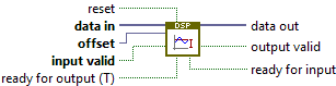
Digital_Offset_Real - 1 spc.vi
Digitally controls the data in offset. This VI must be used in a single-cycle Timed Loop.
This VI provides the following functionality:
data out <= data in + offset
Data Type
This VI automatically adapts to real or complex data in types. It also automatically adapts to the data in array size. Arrays represent parallel samples from one data stream. For array sizes greater than one, the first element ('data in'[0]) is the oldest sample in the array.
Overflows
Overflows on data in.overflow are pipelined along with the data path, combined with overflows that occur inside of this VI, and output on data out.overflow.
Reset
Toggle the reset input to TRUE and then FALSE to reset the internal state of this VI. While in reset, ready for input and output valid are FALSE and input valid is ignored. This VI starts a reset operation when the reset input is set to TRUE or when the LabVIEW FPGA reset method is called.
Pipeline Delay
1 single-cycle Timed Loop clock cycles
Approximate resource usage in a Xilinx Kintex 7
Slice flip-flops: 50
Slice LUTs:: 60
Block RAMs (18kb): 0
DSP48E(1)s: 0
Approximate maximum single-cycle Timed Loop clock rate in a Xilinx Kintex 7
160 MHz

Digital_Offset_Real - 2 spc.vi
Digitally controls the data in offset. This VI must be used in a single-cycle Timed Loop.
This VI provides the following functionality:
data out <= data in + offset
Data Type
This VI automatically adapts to real or complex data in types. It also automatically adapts to the data in array size. Arrays represent parallel samples from one data stream. For array sizes greater than one, the first element ('data in'[0]) is the oldest sample in the array.
Overflows
Overflows on data in.overflow are pipelined along with the data path, combined with overflows that occur inside of this VI, and output on data out.overflow.
Reset
Toggle the reset input to TRUE and then FALSE to reset the internal state of this VI. While in reset, ready for input and output valid are FALSE and input valid is ignored. This VI starts a reset operation when the reset input is set to TRUE or when the LabVIEW FPGA reset method is called.
Pipeline Delay
1 single-cycle Timed Loop clock cycles
Approximate resource usage in a Xilinx Kintex 7
Slice flip-flops: 90
Slice LUTs:: 100
Block RAMs (18kb): 0
DSP48E(1)s: 0
Approximate maximum single-cycle Timed Loop clock rate in a Xilinx Kintex 7
160 MHz
Digital_Offset_Real - 4 spc.vi
Digitally controls the data in offset. This VI must be used in a single-cycle Timed Loop.
This VI provides the following functionality:
data out <= data in + offset
Data Type
This VI automatically adapts to real or complex data in types. It also automatically adapts to the data in array size. Arrays represent parallel samples from one data stream. For array sizes greater than one, the first element ('data in'[0]) is the oldest sample in the array.
Overflows
Overflows on data in.overflow are pipelined along with the data path, combined with overflows that occur inside of this VI, and output on data out.overflow.
Reset
Toggle the reset input to TRUE and then FALSE to reset the internal state of this VI. While in reset, ready for input and output valid are FALSE and input valid is ignored. This VI starts a reset operation when the reset input is set to TRUE or when the LabVIEW FPGA reset method is called.
Pipeline Delay
1 single-cycle Timed Loop clock cycles
Approximate resource usage in a Xilinx Kintex 7
Slice flip-flops: 170
Slice LUTs:: 200
Block RAMs (18kb): 0
DSP48E(1)s: 0
Approximate maximum single-cycle Timed Loop clock rate in a Xilinx Kintex 7
160 MHz

Digital_Offset_Real - 8 spc.vi
Digitally controls the data in offset. This VI must be used in a single-cycle Timed Loop.
This VI provides the following functionality:
data out <= data in + offset
Data Type
This VI automatically adapts to real or complex data in types. It also automatically adapts to the data in array size. Arrays represent parallel samples from one data stream. For array sizes greater than one, the first element ('data in'[0]) is the oldest sample in the array.
Overflows
Overflows on data in.overflow are pipelined along with the data path, combined with overflows that occur inside of this VI, and output on data out.overflow.
Reset
Toggle the reset input to TRUE and then FALSE to reset the internal state of this VI. While in reset, ready for input and output valid are FALSE and input valid is ignored. This VI starts a reset operation when the reset input is set to TRUE or when the LabVIEW FPGA reset method is called.
Pipeline Delay
1 single-cycle Timed Loop clock cycles
Approximate resource usage in a Xilinx Kintex 7
Slice flip-flops: 330
Slice LUTs:: 390
Block RAMs (18kb): 0
DSP48E(1)s: 0
Approximate maximum single-cycle Timed Loop clock rate in a Xilinx Kintex 7
160 MHz

Digital_Offset_Real - 16 spc.vi
Digitally controls the data in offset. This VI must be used in a single-cycle Timed Loop.
This VI provides the following functionality:
data out <= data in + offset
Data Type
This VI automatically adapts to real or complex data in types. It also automatically adapts to the data in array size. Arrays represent parallel samples from one data stream. For array sizes greater than one, the first element ('data in'[0]) is the oldest sample in the array.
Overflows
Overflows on data in.overflow are pipelined along with the data path, combined with overflows that occur inside of this VI, and output on data out.overflow.
Reset
Toggle the reset input to TRUE and then FALSE to reset the internal state of this VI. While in reset, ready for input and output valid are FALSE and input valid is ignored. This VI starts a reset operation when the reset input is set to TRUE or when the LabVIEW FPGA reset method is called.
Pipeline Delay
1 single-cycle Timed Loop clock cycles
Approximate resource usage in a Xilinx Kintex 7
Slice flip-flops: 650
Slice LUTs:: 770
Block RAMs (18kb): 0
DSP48E(1)s: 0
Approximate maximum single-cycle Timed Loop clock rate in a Xilinx Kintex 7
160 MHz

Digital_Offset_1 spc.vi
Digitally controls the I and Q offset. This VI must be used in a single-cycle Timed Loop.
This VI provides the following functionality:
data out.I <= data in.I + offset I
data out.Q <= data in.Q + offset Q
Data Type
This VI automatically adapts to real or complex data in types. It also automatically adapts to the data in array size. Arrays represent parallel samples from one data stream. For array sizes greater than one, the first element ('data in'[0]) is the oldest sample in the array.
Overflows
Overflows on data in.overflow are pipelined along with the data path, combined with overflows that occur inside of this VI, and output on data out.overflow.
Reset
Toggle the reset input to TRUE and then FALSE to reset the internal state of this VI. While in reset, ready for input and output valid are FALSE and input valid is ignored. This VI starts a reset operation when the reset input is set to TRUE or when the LabVIEW FPGA reset method is called.
Pipeline Delay
1 single-cycle Timed Loop clock cycles
Approximate resource usage in a Xilinx Virtex-5 or Virtex-6
Slice flip-flops: 100
Slice LUTs:: 125
Block RAMs (18kb): 0
DSP48E(1)s: 0
Approximate maximum single-cycle Timed Loop clock rate in a Xilinx Virtex-5 or Virtex-6 (-1)
160 MHz

Digital_Offset_2 spc.vi
Digitally controls the I and Q offset. This VI must be used in a single-cycle Timed Loop.
This VI provides the following functionality:
data out.I <= data in.I + offset I
data out.Q <= data in.Q + offset Q
Data Type
This VI automatically adapts to real or complex data in types. It also automatically adapts to the data in array size. Arrays represent parallel samples from one data stream. For array sizes greater than one, the first element ('data in'[0]) is the oldest sample in the array.
Overflows
Overflows on data in.overflow are pipelined along with the data path, combined with overflows that occur inside of this VI, and output on data out.overflow.
Reset
Toggle the reset input to TRUE and then FALSE to reset the internal state of this VI. While in reset, ready for input and output valid are FALSE and input valid is ignored. This VI starts a reset operation when the reset input is set to TRUE or when the LabVIEW FPGA reset method is called.
Pipeline Delay
1 single-cycle Timed Loop clock cycles
Approximate resource usage in a Xilinx Virtex-5 or Virtex-6
Slice flip-flops: 175
Slice LUTs:: 250
Block RAMs (18kb): 0
DSP48E(1)s: 0
Approximate maximum single-cycle Timed Loop clock rate in a Xilinx Virtex-5 or Virtex-6 (-1)
160 MHz

Digital_Offset_4 spc.vi
Digitally controls the I and Q offset. This VI must be used in a single-cycle Timed Loop.
This VI provides the following functionality:
data out.I <= data in.I + offset I
data out.Q <= data in.Q + offset Q
Data Type
This VI automatically adapts to real or complex data in types. It also automatically adapts to the data in array size. Arrays represent parallel samples from one data stream. For array sizes greater than one, the first element ('data in'[0]) is the oldest sample in the array.
Overflows
Overflows on data in.overflow are pipelined along with the data path, combined with overflows that occur inside of this VI, and output on data out.overflow.
Reset
Toggle the reset input to TRUE and then FALSE to reset the internal state of this VI. While in reset, ready for input and output valid are FALSE and input valid is ignored. This VI starts a reset operation when the reset input is set to TRUE or when the LabVIEW FPGA reset method is called.
Pipeline Delay
1 single-cycle Timed Loop clock cycles
Approximate resource usage in a Xilinx Virtex-5 or Virtex-6
Slice flip-flops: 325
Slice LUTs:: 450
Block RAMs (18kb): 0
DSP48E(1)s: 0
Approximate maximum single-cycle Timed Loop clock rate in a Xilinx Virtex-5 or Virtex-6 (-1)
160 MHz

Digital_Offset_8 spc.vi
Digitally controls the I and Q offset. This VI must be used in a single-cycle Timed Loop.
This VI provides the following functionality:
data out.I <= data in.I + offset I
data out.Q <= data in.Q + offset Q
Data Type
This VI automatically adapts to real or complex data in types. It also automatically adapts to the data in array size. Arrays represent parallel samples from one data stream. For array sizes greater than one, the first element ('data in'[0]) is the oldest sample in the array.
Overflows
Overflows on data in.overflow are pipelined along with the data path, combined with overflows that occur inside of this VI, and output on data out.overflow.
Reset
Toggle the reset input to TRUE and then FALSE to reset the internal state of this VI. While in reset, ready for input and output valid are FALSE and input valid is ignored. This VI starts a reset operation when the reset input is set to TRUE or when the LabVIEW FPGA reset method is called.
Pipeline Delay
1 single-cycle Timed Loop clock cycles
Approximate resource usage in a Xilinx Virtex-5 or Virtex-6
Slice flip-flops: 625
Slice LUTs:: 900
Block RAMs (18kb): 0
DSP48E(1)s: 0
Approximate maximum single-cycle Timed Loop clock rate in a Xilinx Virtex-5 or Virtex-6 (-1)
160 MHz

Digital_Offset_16 spc.vi
Digitally controls the I and Q offset. This VI must be used in a single-cycle Timed Loop.
This VI provides the following functionality:
data out.I <= data in.I + offset I
data out.Q <= data in.Q + offset Q
Data Type
This VI automatically adapts to real or complex data in types. It also automatically adapts to the data in array size. Arrays represent parallel samples from one data stream. For array sizes greater than one, the first element ('data in'[0]) is the oldest sample in the array.
Overflows
Overflows on data in.overflow are pipelined along with the data path, combined with overflows that occur inside of this VI, and output on data out.overflow.
Reset
Toggle the reset input to TRUE and then FALSE to reset the internal state of this VI. While in reset, ready for input and output valid are FALSE and input valid is ignored. This VI starts a reset operation when the reset input is set to TRUE or when the LabVIEW FPGA reset method is called.
Pipeline Delay
1 single-cycle Timed Loop clock cycles
Approximate resource usage in a Xilinx Virtex-5 or Virtex-6
Slice flip-flops: 1250
Slice LUTs:: 1800
Block RAMs (18kb): 0
DSP48E(1)s: 0
Approximate maximum single-cycle Timed Loop clock rate in a Xilinx Virtex-5 or Virtex-6 (-1)
160 MHz

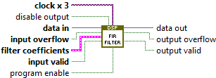
Equalization - 11 cps - 1x oc - 32 coef.vi
Equalizes the analog response of a device. This VI implements four FIR filters as a matrix operation, and can also be used as a general purpose complex filter. This VI must be used in a single-cycle Timed Loop.
This VI provides the following functionality:
data out.I <= data in.I * I Inline - data in.Q * Q Cross
data out.Q <= data in.Q * Q Inline + data in.I * I Cross
Where "*" represents convolution, and I Inline, Q Cross, Q Inline, and I Cross are the sets of coefficients for the four filters.
Data Type
This VI automatically adapts to the data in array size. Arrays represent parallel samples from one data stream. For array sizes greater than one, the first element ('data in'[0]) is the oldest sample in the array.
Throughput
This VI can consume one I/Q sample at most once every eleven single-cycle Timed Loop clock cycles. ready for input will deassert for ten clock cycles after every assertion of input valid.
Overflows
Overflows on data in.overflow are pipelined along with the data path, combined with overflows that occur inside of this VI, and output on data out.overflow.
Reset
Toggle the reset input to TRUE and then FALSE to reset the internal state of this VI. While in reset, ready for input and output valid are FALSE and input valid is ignored. This VI starts a reset operation when the reset input is set to TRUE or when the LabVIEW FPGA reset method is called. A reset operation takes 50 clock cycles to complete. The coefficients are not modified during a reset.
Programming
Each of the four FIR filters has 32 coefficients. The default value for all of the coefficients is 0. There are no requirements to the symmetry of the coefficients. Load the filter coefficients using the filter coefficients input.
For 1 sample per cycle, load the coefficients in natural order (0, 1, 2, 3 ...)
Complete the following steps to load the coefficients:
1. Select the filter to load using filter select.
2. Set coef load to TRUE and then FALSE, to begin the load sequence.
3. For each coefficient: write a coefficient to coef data and set coef write TRUE, then set coef write FALSE.
The new coefficients are applied automatically while they are being written. For the most consistent output behavior, hold the reset input TRUE while loading the coefficients.
You can use the Digital Filter Design Toolkit to calculate coefficients for your desired filtering application.
Pipeline Delay
40 single-cycle Timed Loop clock cycles
Approximate resource usage in a Xilinx Virtex-6
Slice flip-flops: 1000
Slice LUTs:: 1200
Block RAMs (18kb): 0
DSP48E(1)s: 12
Approximate maximum single-cycle Timed Loop clock rate in a Xilinx Virtex-6 (-1)
160 MHz

Equalization - 1 spc - 3x oc - 33 coef.vi
Equalizes the analog response of a device. This VI implements four FIR filters as a matrix operation, and can also be used as a general purpose complex filter. This VI must be used in a single-cycle Timed Loop.
This VI provides the following functionality:
data out.I <= data in.I * I Inline - data in.Q * Q Cross
data out.Q <= data in.Q * Q Inline + data in.I * I Cross
Where "*" represents convolution, and I Inline, Q Cross, Q Inline, and I Cross are the sets of coefficients for the four filters.
Data Type
This VI automatically adapts to the data in array size. Arrays represent parallel samples from one data stream. For array sizes greater than one, the first element ('data in'[0]) is the oldest sample in the array.
Over-clocking
This VI must be used in a single-cycle Timed Loop and requires an additional in-phase clock at three times the frequency of the single-cycle Timed Loop clock.
Overflows
Overflows on data in.overflow are pipelined along with the data path, combined with overflows that occur inside of this VI, and output on data out.overflow.
Reset
Toggle the reset input to TRUE and then FALSE to reset the internal state of this VI. While in reset, ready for input and output valid are FALSE and input valid is ignored. This VI starts a reset operation when the reset input is set to TRUE or when the LabVIEW FPGA reset method is called. A reset operation takes 50 clock cycles to complete. The coefficients are not modified during a reset.
Programming
Each of the four FIR filters has 33 coefficients. The default value for all of the coefficients is 0. There are no requirements to the symmetry of the coefficients. Load the filter coefficients using the filter coefficients input.
For 1 sample per cycle, load the coefficients in natural order (0, 1, 2, 3 ...)
Complete the following steps to load the coefficients:
1. Select the filter to load using filter select.
2. Set coef load to TRUE and then FALSE, to begin the load sequence.
3. For each coefficient: write a coefficient to coef data and set coef write TRUE, then set coef write FALSE.
The new coefficients are applied automatically while they are being written. For the most consistent output behavior, hold the reset input TRUE while loading the coefficients.
You can use the Digital Filter Design Toolkit to calculate coefficients for your desired filtering application.
Pipeline Delay
11 single-cycle Timed Loop clock cycles
Approximate resource usage in a Xilinx Virtex-6
Slice flip-flops: 2850
Slice LUTs:: 1300
Block RAMs (18kb): 0
DSP48E(1)s: 52
Approximate maximum single-cycle Timed Loop clock rate in a Xilinx Virtex-6 (-1)
130 MHz

Equalization - 2 spc - 3x oc - 48 coef.vi
Equalizes the analog response of a device. This VI implements four FIR filters as a matrix operation, and can also be used as a general purpose complex filter. This VI must be used in a single-cycle Timed Loop.
This VI provides the following functionality:
data out.I <= data in.I * I Inline - data in.Q * Q Cross
data out.Q <= data in.Q * Q Inline + data in.I * I Cross
Where "*" represents convolution, and I Inline, Q Cross, Q Inline, and I Cross are the sets of coefficients for the four filters.
Data Type
This VI automatically adapts to the data in array size. Arrays represent parallel samples from one data stream. For array sizes greater than one, the first element ('data in'[0]) is the oldest sample in the array.
Over-clocking
This VI must be used in a single-cycle Timed Loop and requires an additional in-phase clock at three times the frequency of the single-cycle Timed Loop clock.
Overflows
Overflows on data in.overflow are pipelined along with the data path, combined with overflows that occur inside of this VI, and output on data out.overflow.
Reset
Toggle the reset input to TRUE and then FALSE to reset the internal state of this VI. While in reset, ready for input and output valid are FALSE and input valid is ignored. This VI starts a reset operation when the reset input is set to TRUE or when the LabVIEW FPGA reset method is called. A reset operation takes 50 clock cycles to complete. The coefficients are not modified during a reset.
Programming
Each of the four FIR filters has 48 coefficients. The default value for all of the coefficients is 0. There are no requirements to the symmetry of the coefficients. Load the filter coefficients using the filter coefficients input.
For multiple samples per cycle, load the coefficients with an SPC step size, and wrap back to the beginning when you reach the end.
For example, four samples per cycle and 32 coefficients uses the following order:
0, 4, 8, 12, 16, 20, 24, 28, 1, 5, 9, 13, 17, 21, 25, 29, 2, 6, 10, 14, 18, 22, 26, 30, 3, 7, 11, 15, 19, 23, 27, 31
Complete the following steps to load the coefficients:
1. Select the filter to load using filter select.
2. Set coef load to TRUE and then FALSE, to begin the load sequence.
3. For each coefficient: write a coefficient to coef data and set coef write TRUE, then set coef write FALSE.
The new coefficients are applied automatically while they are being written. For the most consistent output behavior, hold the reset input TRUE while loading the coefficients.
You can use the Digital Filter Design Toolkit to calculate coefficients for your desired filtering application.
Pipeline Delay
13 single-cycle Timed Loop clock cycles
Approximate resource usage in a Xilinx Virtex-6
Slice flip-flops: 8100
Slice LUTs:: 3650
Block RAMs (18kb): 0
DSP48E(1)s: 144
Approximate maximum single-cycle Timed Loop clock rate in a Xilinx Virtex-6 (-1)
130 MHz

Equalization - 4 spc - 2x oc - 32 coef.vi
Equalizes the analog response of a device. This VI implements four FIR filters as a matrix operation, and can also be used as a general purpose complex filter. This VI must be used in a single-cycle Timed Loop.
This VI provides the following functionality:
data out.I <= data in.I * I Inline - data in.Q * Q Cross
data out.Q <= data in.Q * Q Inline + data in.I * I Cross
Where "*" represents convolution, and I Inline, Q Cross, Q Inline, and I Cross are the sets of coefficients for the four filters.
Data Type
This VI automatically adapts to the data in array size. Arrays represent parallel samples from one data stream. For array sizes greater than one, the first element ('data in'[0]) is the oldest sample in the array.
Over-clocking
This VI must be used in a single-cycle Timed Loop and requires an additional in-phase clock at two times the frequency of the single-cycle Timed Loop clock.
Overflows
Overflows on data in.overflow are pipelined along with the data path, combined with overflows that occur inside of this VI, and output on data out.overflow.
Reset
Toggle the reset input to TRUE and then FALSE to reset the internal state of this VI. While in reset, ready for input and output valid are FALSE and input valid is ignored. This VI starts a reset operation when the reset input is set to TRUE or when the LabVIEW FPGA reset method is called. A reset operation takes 50 clock cycles to complete. The coefficients are not modified during a reset.
Programming
Each of the four FIR filters has 32 coefficients. The default value for all of the coefficients is 0. There are no requirements to the symmetry of the coefficients. Load the filter coefficients using the filter coefficients input.
For multiple samples per cycle, load the coefficients with an SPC step size, and wrap back to the beginning when you reach the end.
For example, four samples per cycle and 32 coefficients uses the following order:
0, 4, 8, 12, 16, 20, 24, 28, 1, 5, 9, 13, 17, 21, 25, 29, 2, 6, 10, 14, 18, 22, 26, 30, 3, 7, 11, 15, 19, 23, 27, 31
Complete the following steps to load the coefficients:
1. Select the filter to load using filter select.
2. Set coef load to TRUE and then FALSE, to begin the load sequence.
3. For each coefficient: write a coefficient to coef data and set coef write TRUE, then set coef write FALSE.
The new coefficients are applied automatically while they are being written. For the most consistent output behavior, hold the reset input TRUE while loading the coefficients.
You can use the Digital Filter Design Toolkit to calculate coefficients for your desired filtering application.
Pipeline Delay
17 single-cycle Timed Loop clock cycles
Approximate resource usage in a Xilinx Virtex-6
Slice flip-flops: 16500
Slice LUTs:: 7550
Block RAMs (18kb): 0
DSP48E(1)s: 288
Approximate maximum single-cycle Timed Loop clock rate in a Xilinx Virtex-6 (-1)
130 MHz

Equalization - 8 spc - 2x oc - 32 coef.vi
Equalizes the analog response of a device. This VI implements four FIR filters as a matrix operation, and can also be used as a general purpose complex filter. This VI must be used in a single-cycle Timed Loop.
This VI provides the following functionality:
data out.I <= data in.I * I Inline - data in.Q * Q Cross
data out.Q <= data in.Q * Q Inline + data in.I * I Cross
Where "*" represents convolution, and I Inline, Q Cross, Q Inline, and I Cross are the sets of coefficients for the four filters.
Data Type
This VI automatically adapts to the data in array size. Arrays represent parallel samples from one data stream. For array sizes greater than one, the first element ('data in'[0]) is the oldest sample in the array.
Over-clocking
This VI must be used in a single-cycle Timed Loop and requires an additional in-phase clock at two times the frequency of the single-cycle Timed Loop clock.
Overflows
Overflows on data in.overflow are pipelined along with the data path, combined with overflows that occur inside of this VI, and output on data out.overflow.
Reset
Toggle the reset input to TRUE and then FALSE to reset the internal state of this VI. While in reset, ready for input and output valid are FALSE and input valid is ignored. This VI starts a reset operation when the reset input is set to TRUE or when the LabVIEW FPGA reset method is called. A reset operation takes 50 clock cycles to complete. The coefficients are not modified during a reset.
Programming
Each of the four FIR filters has 32 coefficients. The default value for all of the coefficients is 0. There are no requirements to the symmetry of the coefficients. Load the filter coefficients using the filter coefficients input.
For multiple samples per cycle, load the coefficients with an SPC step size, and wrap back to the beginning when you reach the end.
For example, four samples per cycle and 32 coefficients uses the following order:
0, 4, 8, 12, 16, 20, 24, 28, 1, 5, 9, 13, 17, 21, 25, 29, 2, 6, 10, 14, 18, 22, 26, 30, 3, 7, 11, 15, 19, 23, 27, 31
Complete the following steps to load the coefficients:
1. Select the filter to load using filter select.
2. Set coef load to TRUE and then FALSE, to begin the load sequence.
3. For each coefficient: write a coefficient to coef data and set coef write TRUE, then set coef write FALSE.
The new coefficients are applied automatically while they are being written. For the most consistent output behavior, hold the reset input TRUE while loading the coefficients.
You can use the Digital Filter Design Toolkit to calculate coefficients for your desired filtering application.
Pipeline Delay
17 single-cycle Timed Loop clock cycles
Approximate resource usage in a Xilinx Virtex-6
Slice flip-flops: 35500
Slice LUTs:: 16900
Block RAMs (18kb): 0
DSP48E(1)s: 576
Approximate maximum single-cycle Timed Loop clock rate in a Xilinx Virtex-6 (-1)
130 MHz

Halfband Decimator - IQ - 4 CPS - 2x OC.vi
Decimates the input signal data in by a factor of two using a low-pass halfband FIR filter implementation. This VI must be used in a single-cycle Timed Loop.
Data Type
This VI automatically adapts to the data in array size. Arrays represent parallel samples from one data stream. For array sizes greater than one, the first element ('data in'[0]) is the oldest sample in the array.
Throughput
This VI can consume one I/Q sample at most once every four single-cycle Timed Loop clock cycles. ready for input will deassert for three clock cycles after every assertion of input valid.
Over-clocking
This VI must be used in a single-cycle Timed Loop and requires an additional in-phase clock at two times the frequency of the single-cycle Timed Loop clock.
Overflows
Overflows on data in.overflow are pipelined along with the data path, combined with overflows that occur inside of this VI, and output on data out.overflow.
Reset
Toggle the reset input to TRUE and then FALSE to reset the internal state of this VI. While in reset, ready for input and output valid are FALSE and input valid is ignored. This VI starts a reset operation when the reset input is set to TRUE or when the LabVIEW FPGA reset method is called. A reset operation takes 100 clock cycles to complete.
Pipeline Delay
The pipeline delay from the first input valid to the first output valid is 14 single-cycle Timed Loop clock cycles.
Group delay
14.5 output samples.
Performance
Decimation Factor: 2
Anti-alias low-pass filter passband ripple (to 0.4 * output data rate): 0 dB to -0.01 dB
Anti-alias low-pass filter stopband rejection (from 0.6 * output data rate): > 85 dB
Approximate resource usage in a Xilinx Virtex-6
Slice flip-flops: 550
Slice LUTs: 350
Block RAMs (18kb): 0
DSP48E(1)s: 2
Approximate maximum single-cycle Timed Loop clock rate in a Xilinx Virtex-6 (-1)
160 MHz

Halfband Decimator - IQ - 2 CPS - 2x OC.vi
Decimates the input signal data in by a factor of two using a low-pass halfband FIR filter implementation. This VI must be used in a single-cycle Timed Loop.
Data Type
This VI automatically adapts to the data in array size. Arrays represent parallel samples from one data stream. For array sizes greater than one, the first element ('data in'[0]) is the oldest sample in the array.
Throughput
This VI can consume one I/Q sample at most once every two single-cycle Timed Loop clock cycles. ready for input will deassert for one clock cycles after every assertion of input valid.
Over-clocking
This VI must be used in a single-cycle Timed Loop and requires an additional in-phase clock at two times the frequency of the single-cycle Timed Loop clock.
Overflows
Overflows on data in.overflow are pipelined along with the data path, combined with overflows that occur inside of this VI, and output on data out.overflow.
Reset
Toggle the reset input to TRUE and then FALSE to reset the internal state of this VI. While in reset, ready for input and output valid are FALSE and input valid is ignored. This VI starts a reset operation when the reset input is set to TRUE or when the LabVIEW FPGA reset method is called. A reset operation takes 100 clock cycles to complete.
Pipeline Delay
The pipeline delay from the first input valid to the first output valid is 14 single-cycle Timed Loop clock cycles.
Group delay
14.5 output samples.
Performance
Decimation Factor: 2
Anti-alias low-pass filter passband ripple (to 0.4 * output data rate): 0 dB to -0.01 dB
Anti-alias low-pass filter stopband rejection (from 0.6 * output data rate): > 85 dB
Approximate resource usage in a Xilinx Virtex-6
Slice flip-flops: 800
Slice LUTs:: 500
Block RAMs (18kb): 0
DSP48E(1)s: 4
Approximate maximum single-cycle Timed Loop clock rate in a Xilinx Virtex-6 (-1)
160 MHz

Halfband Decimator - IQ - 1 SPC - 2x OC.vi
Decimates the input signal data in by a factor of two using a low-pass halfband FIR filter implementation. This VI must be used in a single-cycle Timed Loop.
Data Type
This VI automatically adapts to the data in array size. Arrays represent parallel samples from one data stream. For array sizes greater than one, the first element ('data in'[0]) is the oldest sample in the array.
Over-clocking
This VI must be used in a single-cycle Timed Loop and requires an additional in-phase clock at two times the frequency of the single-cycle Timed Loop clock.
Overflows
Overflows on data in.overflow are pipelined along with the data path, combined with overflows that occur inside of this VI, and output on data out.overflow.
Reset
Toggle the reset input to TRUE and then FALSE to reset the internal state of this VI. While in reset, ready for input and output valid are FALSE and input valid is ignored. This VI starts a reset operation when the reset input is set to TRUE or when the LabVIEW FPGA reset method is called. A reset operation takes 100 clock cycles to complete.
Pipeline Delay
The pipeline delay from the first input valid to the first output valid is 14 single-cycle Timed Loop clock cycles.
Group delay
14.5 output samples.
Performance
Decimation Factor: 2
Anti-alias low-pass filter passband ripple (to 0.4 * output data rate): 0 dB to -0.01 dB
Anti-alias low-pass filter stopband rejection (from 0.6 * output data rate): > 85 dB
Approximate resource usage in a Xilinx Virtex-6
Slice flip-flops: 1200
Slice LUTs:: 800
Block RAMs (18kb): 0
DSP48E(1)s: 8
Approximate maximum single-cycle Timed Loop clock rate in a Xilinx Virtex-6 (-1)
160 MHz

Halfband Decimator - IQ - 2 spc - 2x oc.vi
Decimates the input signal data in by a factor of two using a low-pass halfband FIR filter implementation. This VI must be used in a single-cycle Timed Loop.
Data Type
This VI automatically adapts to the data in array size. Arrays represent parallel samples from one data stream. For array sizes greater than one, the first element ('data in'[0]) is the oldest sample in the array.
Over-clocking
This VI must be used in a single-cycle Timed Loop and requires an additional in-phase clock at two times the frequency of the single-cycle Timed Loop clock.
Overflows
Overflows on data in.overflow are pipelined along with the data path, combined with overflows that occur inside of this VI, and output on data out.overflow.
Reset
Toggle the reset input to TRUE and then FALSE to reset the internal state of this VI. While in reset, ready for input and output valid are FALSE and input valid is ignored. This VI starts a reset operation when the reset input is set to TRUE or when the LabVIEW FPGA reset method is called. A reset operation takes 100 clock cycles to complete.
Pipeline Delay
The pipeline delay from the first input valid to the first output valid is 14 single-cycle Timed Loop clock cycles.
Group delay
14.5 output samples.
Performance
Decimation Factor: 2
Anti-alias low-pass filter passband ripple (to 0.4 * output data rate): 0 dB to -0.01 dB
Anti-alias low-pass filter stopband rejection (from 0.6 * output data rate): > 85 dB
Approximate resource usage in a Xilinx Virtex-6
Slice flip-flops: 2000
Slice LUTs:: 1300
Block RAMs (18kb): 0
DSP48E(1)s: 16
Approximate maximum single-cycle Timed Loop clock rate in a Xilinx Virtex-6 (-1)
160 MHz

Halfband Decimator - IQ - 4 spc - 2x oc.vi
Decimates the input signal data in by a factor of two using a low-pass halfband FIR filter implementation. This VI must be used in a single-cycle Timed Loop.
Data Type
This VI automatically adapts to the data in array size. Arrays represent parallel samples from one data stream. For array sizes greater than one, the first element ('data in'[0]) is the oldest sample in the array.
Over-clocking
This VI must be used in a single-cycle Timed Loop and requires an additional in-phase clock at two times the frequency of the single-cycle Timed Loop clock.
Overflows
Overflows on data in.overflow are pipelined along with the data path, combined with overflows that occur inside of this VI, and output on data out.overflow.
Reset
Toggle the reset input to TRUE and then FALSE to reset the internal state of this VI. While in reset, ready for input and output valid are FALSE and input valid is ignored. This VI starts a reset operation when the reset input is set to TRUE or when the LabVIEW FPGA reset method is called. A reset operation takes 100 clock cycles to complete.
Pipeline Delay
The pipeline delay from the first input valid to the first output valid is 14 single-cycle Timed Loop clock cycles.
Group delay
14.5 output samples.
Performance
Decimation Factor: 2
Anti-alias low-pass filter passband ripple (to 0.4 * output data rate): 0 dB to -0.01 dB
Anti-alias low-pass filter stopband rejection (from 0.6 * output data rate): > 85 dB
Approximate resource usage in a Xilinx Virtex-6
Slice flip-flops: 3800
Slice LUTs:: 2500
Block RAMs (18kb): 0
DSP48E(1)s: 32
Approximate maximum single-cycle Timed Loop clock rate in a Xilinx Virtex-6 (-1)
160 MHz

Halfband Decimator - IQ - 8 spc - 2x oc.vi
Decimates the input signal data in by a factor of two using a low-pass halfband FIR filter implementation. This VI must be used in a single-cycle Timed Loop.
Data Type
This VI automatically adapts to the data in array size. Arrays represent parallel samples from one data stream. For array sizes greater than one, the first element ('data in'[0]) is the oldest sample in the array.
Over-clocking
This VI must be used in a single-cycle Timed Loop and requires an additional in-phase clock at two times the frequency of the single-cycle Timed Loop clock.
Overflows
Overflows on data in.overflow are pipelined along with the data path, combined with overflows that occur inside of this VI, and output on data out.overflow.
Reset
Toggle the reset input to TRUE and then FALSE to reset the internal state of this VI. While in reset, ready for input and output valid are FALSE and input valid is ignored. This VI starts a reset operation when the reset input is set to TRUE or when the LabVIEW FPGA reset method is called. A reset operation takes 100 clock cycles to complete.
Pipeline Delay
The pipeline delay from the first input valid to the first output valid is 14 single-cycle Timed Loop clock cycles.
Group delay
14.5 output samples.
Performance
Decimation Factor: 2
Anti-alias low-pass filter passband ripple (to 0.4 * output data rate): 0 dB to -0.01 dB
Anti-alias low-pass filter stopband rejection (from 0.6 * output data rate): > 85 dB
Approximate resource usage in a Xilinx Virtex-6
Slice flip-flops: 7400
Slice LUTs:: 4800
Block RAMs (18kb): 0
DSP48E(1)s: 64
Approximate maximum single-cycle Timed Loop clock rate in a Xilinx Virtex-6 (-1)
160 MHz

Halfband Decimator - IQ - 16 spc - 2x oc.vi
Decimates the input signal data in by a factor of two using a low-pass halfband FIR filter implementation. This VI must be used in a single-cycle Timed Loop.
Data Type
This VI automatically adapts to the data in array size. Arrays represent parallel samples from one data stream. For array sizes greater than one, the first element ('data in'[0]) is the oldest sample in the array.
Over-clocking
This VI must be used in a single-cycle Timed Loop and requires an additional in-phase clock at two times the frequency of the single-cycle Timed Loop clock.
Overflows
Overflows on data in.overflow are pipelined along with the data path, combined with overflows that occur inside of this VI, and output on data out.overflow.
Reset
Toggle the reset input to TRUE and then FALSE to reset the internal state of this VI. While in reset, ready for input and output valid are FALSE and input valid is ignored. This VI starts a reset operation when the reset input is set to TRUE or when the LabVIEW FPGA reset method is called. A reset operation takes 100 clock cycles to complete.
Pipeline Delay
The pipeline delay from the first input valid to the first output valid is 14 single-cycle Timed Loop clock cycles.
Group delay
14.5 output samples.
Performance
Decimation Factor: 2
Anti-alias low-pass filter passband ripple (to 0.4 * output data rate): 0 dB to -0.01 dB
Anti-alias low-pass filter stopband rejection (from 0.6 * output data rate): > 85 dB
Approximate resource usage in a Xilinx Virtex-6
Slice flip-flops: 14500
Slice LUTs:: 9300
Block RAMs (18kb): 0
DSP48E(1)s: 128
Approximate maximum single-cycle Timed Loop clock rate in a Xilinx Virtex-6 (-1)
160 MHz

Integer Decimator - real - NAP - 2 spc.vi
Decimates the input signal data in by an integer decimation factor, without filtering for alias protection. This VI must be used in a single-cycle Timed Loop.
Data Type
This VI automatically adapts to the data in array size. Arrays represent parallel samples from one data stream. For array sizes greater than one, the first element ('data in'[0]) is the oldest sample in the array.
decimation factor
This signal specifies the decimation factor and its acceptable range is 0 to 65,535. Decimation is performed by discarding input data based on the value specified in this signal. When decimation factor is set to 0 or 1, no decimation is performed. For example, when decimation factor is 4, every fourth input data is output.
Reset
Toggle the reset input to TRUE and then FALSE to reset the internal state of this VI. While in reset, ready for input and output valid are FALSE and input valid is ignored. This VI starts a reset operation when the reset input is set to TRUE or when the LabVIEW FPGA reset method is called. An internal reset is initiated any time the decimation factor changes.
output calculated
This signal provides information on which input data is part of the decimated data. For example, for a data in array size of two, when output calculated = FT (FALSE, True), input data in[0] is part of the decimation data. When output calculated = FF, no input data in the current clock is part of the decimated data. This signal has the same number of pipeline stages as the data path.
Pipeline Delay
2 single-cycle Timed Loop clock cycles
Approximate resource usage in a Xilinx Kintex 7
Slice flip-flops: 151
Slice LUTs:: 99
Block RAMs (18kb): 0
DSP48E(1)s: 0
Approximate maximum single-cycle Timed Loop clock rate in a Xilinx Kintex 7
180 MHz

Fractional Decimator - 10 cps - 1x oc.vi
Decimates the input signal data in according to the output sample rate and delay using an FIR filter implementation. This VI must be used in a single-cycle Timed Loop.
Data Type
This VI automatically adapts to the data in array size. Arrays represent parallel samples from one data stream. For array sizes greater than one, the first element ('data in'[0]) is the oldest sample in the array.
Throughput
This VI can consume one I/Q sample at most once every ten single-cycle Timed Loop clock cycles. ready for input will deassert for nine clock cycles after every assertion of input valid.
Data Rate
The output sample rate input may be in the range of [1.52588E-5 to 1.0]. This corresponds to decimation factors of [65,536.0 down to 1.0]. It produces data out outputs at a sample rate equal to the normalized output sample rate.
decimation factor = 1 / output sample rate
output data rate (in Hz) = input data rate (in Hz) * output sample rate
The input data rate is defined by the clock frequency of the single-cycle Timed Loop (SCTL), the number of samples per cycle (SPC) in data in, and the fraction of cycles on which input valid is asserted.
input data rate = SCTL clock frequency * SPC * fraction of cycles on which input valid is asserted
For example if the SCTL is clocked at 120 MHz, one SPC is used, and the input valid signal is asserted on every other cycle, then the input data rate is 60 MHz.
Delay
The delay input delays the input data. The valid range for delay is [-0.5 to +0.5].
delay (in seconds) = delay / input data rate (in Hz)
Overflows
Overflows on data in.overflow are pipelined along with the data path, combined with overflows that occur inside of this VI, and output on data out.overflow.
Reset
Toggle the reset input to TRUE and then FALSE to reset the internal state of this VI. While in reset, ready for input and output valid are FALSE and input valid is ignored. This VI starts a reset operation when the reset input is set to TRUE or when the LabVIEW FPGA reset method is called. A reset operation takes 1100 clock cycles to complete. An internal reset is initiated any time the output sample rate changes.
Pipeline Delay
The pipeline delay from the first input valid to the first output valid varies between 49 and 1599, depending on the output sample rate value.
Group delay of the anti-alias filter
decimation factor <= 16: group delay = 15 output samples
16 < decimation factor <= 128: group delay = (256 / decimation factor) + 15 output samples
128 < decimation factor <= 2,048: group delay = (2,056 / decimation factor) + 15 output samples
2,048 < decimation factor <= 32,768: group delay = (34,624 / decimation factor) + 15 output samples
32,768 < decimation factor <= 65,536: group delay (65,344 / decimation factor) + 15 output samples
Performance
Decimation Range: [1.0 to 65,536.0]
Output Sample Rate Resolution: 7.11e-15 * input data rate (in Hz)
Delay Range: [-0.5 to +0.5] (corresponds to -0.5 to +0.5 input data rate periods)
Delay Resolution: 1.53e-5 / input data rate (in Hz)
Anti-alias filter passband ripple (to 0.4 * output data rate): 0 dB to -0.01 dB
Anti-alias filter stopband rejection(from 0.6 * output data rate): > 85 dB
Approximate resource usage in a Xilinx Virtex-6
Slice flip-flops: 2800
Slice LUTs:: 6100
Block RAMs (18kb): 25
DSP48E(1)s: 34
Approximate maximum single-cycle Timed Loop clock rate in a Xilinx Virtex-6 (-1)
xxx MHz

Fractional Decimator - 1 spc - 2x oc.vi
Decimates the input signal data in according to the output sample rate and delay using an FIR filter implementation. This VI must be used in a single-cycle Timed Loop.
Data Type
This VI automatically adapts to the data in array size. Arrays represent parallel samples from one data stream. For array sizes greater than one, the first element ('data in'[0]) is the oldest sample in the array.
Over-clocking
This VI must be used in a single-cycle Timed Loop and requires an additional in-phase clock at two times the frequency of the single-cycle Timed Loop clock.
Data Rate
The output sample rate input may be in the range of [1.52588E-5 to 1.0]. This corresponds to decimation factors of [65,536.0 down to 1.0]. It produces data out outputs at a sample rate equal to the normalized output sample rate.
decimation factor = 1 / output sample rate
output data rate (in Hz) = input data rate (in Hz) * output sample rate
The input data rate is defined by the clock frequency of the single-cycle Timed Loop (SCTL), the number of samples per cycle (SPC) in data in, and the fraction of cycles on which input valid is asserted.
input data rate = SCTL clock frequency * SPC * fraction of cycles on which input valid is asserted
For example if the SCTL is clocked at 120 MHz, one SPC is used, and the input valid signal is asserted on every other cycle, then the input data rate is 60 MHz.
Delay
The delay input delays the input data. The valid range for delay is [-0.5 to +0.5].
delay (in seconds) = delay / input data rate (in Hz)
Overflows
Overflows on data in.overflow are pipelined along with the data path, combined with overflows that occur inside of this VI, and output on data out.overflow.
Reset
Toggle the reset input to TRUE and then FALSE to reset the internal state of this VI. While in reset, ready for input and output valid are FALSE and input valid is ignored. This VI starts a reset operation when the reset input is set to TRUE or when the LabVIEW FPGA reset method is called. A reset operation takes 1100 clock cycles to complete. An internal reset is initiated any time the output sample rate changes.
Pipeline Delay
The pipeline delay from the first input valid to the first output valid varies between 33 and 827, depending on the output sample rate value.
Group delay of the anti-alias filter
decimation factor <= 16: group delay = 15 output samples
16 < decimation factor <= 128: group delay = (256 / decimation factor) + 15 output samples
128 < decimation factor <= 2,048: group delay = (2,056 / decimation factor) + 15 output samples
2,048 < decimation factor <= 32,768: group delay = (34,624 / decimation factor) + 15 output samples
32,768 < decimation factor <= 65,536: group delay (65,344 / decimation factor) + 15 output samples
Performance
Decimation Range: [1.0 to 65,536.0]
Output Sample Rate Resolution: 7.11e-15 * input data rate (in Hz)
Delay Range: [-0.5 to +0.5] (corresponds to -0.5 to +0.5 input data rate periods)
Delay Resolution: 1.53e-5 / input data rate (in Hz)
Anti-alias filter passband ripple (to 0.4 * output data rate): 0 dB to -0.01 dB
Anti-alias filter stopband rejection(from 0.6 * output data rate): > 85 dB
Approximate resource usage in a Xilinx Virtex-6
Slice flip-flops: 10300
Slice LUTs:: 6100
Block RAMs (18kb): 77
DSP48E(1)s: 72
Approximate maximum single-cycle Timed Loop clock rate in a Xilinx Virtex-6 (-1)
160 MHz

Fractional Decimator - 1 spc - 3x oc.vi
Decimates the input signal data in according to the output sample rate and delay using an FIR filter implementation. This VI must be used in a single-cycle Timed Loop.
Data Type
This VI automatically adapts to the data in array size. Arrays represent parallel samples from one data stream. For array sizes greater than one, the first element ('data in'[0]) is the oldest sample in the array.
Over-clocking
This VI must be used in a single-cycle Timed Loop and requires an additional in-phase clock at three times the frequency of the single-cycle Timed Loop clock.
Data Rate
The output sample rate input may be in the range of [1.52588E-5 to 1.0]. This corresponds to decimation factors of [65,536.0 down to 1.0]. It produces data out outputs at a sample rate equal to the normalized output sample rate.
decimation factor = 1 / output sample rate
output data rate (in Hz) = input data rate (in Hz) * output sample rate
The input data rate is defined by the clock frequency of the single-cycle Timed Loop (SCTL), the number of samples per cycle (SPC) in data in, and the fraction of cycles on which input valid is asserted.
input data rate = SCTL clock frequency * SPC * fraction of cycles on which input valid is asserted
For example if the SCTL is clocked at 120 MHz, one SPC is used, and the input valid signal is asserted on every other cycle, then the input data rate is 60 MHz.
Delay
The delay input delays the input data. The valid range for delay is [-0.5 to +0.5].
delay (in seconds) = delay / input data rate (in Hz)
Overflows
Overflows on data in.overflow are pipelined along with the data path, combined with overflows that occur inside of this VI, and output on data out.overflow.
Reset
Toggle the reset input to TRUE and then FALSE to reset the internal state of this VI. While in reset, ready for input and output valid are FALSE and input valid is ignored. This VI starts a reset operation when the reset input is set to TRUE or when the LabVIEW FPGA reset method is called. A reset operation takes 1100 clock cycles to complete. An internal reset is initiated any time the output sample rate changes.
Pipeline Delay
The pipeline delay from the first input valid to the first output valid varies between 25 and 559, depending on the output sample rate value.
Group delay of the anti-alias filter
decimation factor <= 16: group delay = 15 output samples
16 < decimation factor <= 128: group delay = (256 / decimation factor) + 15 output samples
128 < decimation factor <= 2,048: group delay = (2,056 / decimation factor) + 15 output samples
2,048 < decimation factor <= 32,768: group delay = (34,624 / decimation factor) + 15 output samples
32,768 < decimation factor <= 65,536: group delay (65,344 / decimation factor) + 15 output samples
Performance
Decimation Range: [1.0 to 65,536.0]
Output Sample Rate Resolution: 7.11e-15 * input data rate (in Hz)
Delay Range: [-0.5 to +0.5] (corresponds to -0.5 to +0.5 input data rate periods)
Delay Resolution: 1.53e-5 / input data rate (in Hz)
Anti-alias filter passband ripple (to 0.4 * output data rate): 0 dB to -0.01 dB
Anti-alias filter stopband rejection(from 0.6 * output data rate): > 85 dB
Approximate resource usage in a Xilinx Virtex-6
Slice flip-flops: 7700
Slice LUTs:: 4900
Block RAMs (18kb): 50
DSP48E(1)s: 50
Approximate maximum single-cycle Timed Loop clock rate in a Xilinx Virtex-6 (-1)
125 MHz

Fractional Decimator - 2 spc - 2x oc.vi
Decimates the input signal data in according to the output sample rate and delay using an FIR filter implementation. This VI must be used in a single-cycle Timed Loop.
Data Type
This VI automatically adapts to the data in array size. Arrays represent parallel samples from one data stream. For array sizes greater than one, the first element ('data in'[0]) is the oldest sample in the array.
Over-clocking
This VI must be used in a single-cycle Timed Loop and requires an additional in-phase clock at two times the frequency of the single-cycle Timed Loop clock.
Data Rate
The output sample rate input may be in the range of [1.52588E-5 to 1.0]. This corresponds to decimation factors of [65,536.0 down to 1.0]. It produces data out outputs at a sample rate equal to the normalized output sample rate.
decimation factor = 1 / output sample rate
output data rate (in Hz) = input data rate (in Hz) * output sample rate
The input data rate is defined by the clock frequency of the single-cycle Timed Loop (SCTL), the number of samples per cycle (SPC) in data in, and the fraction of cycles on which input valid is asserted.
input data rate = SCTL clock frequency * SPC * fraction of cycles on which input valid is asserted
For example if the SCTL is clocked at 120 MHz, one SPC is used, and the input valid signal is asserted on every other cycle, then the input data rate is 60 MHz.
Delay
The delay input delays the input data. The valid range for delay is [-0.5 to +0.5].
delay (in seconds) = delay / input data rate (in Hz)
Output Calculated
Output calculated indicates when a new output sample has been calculated in the decimator and points to the last input sample used in the convolution to calculate the output sample. In contrast, output valid asserts only when all of the samples on data out are valid.
Overflows
Overflows on data in.overflow are pipelined along with the data path, combined with overflows that occur inside of this VI, and output on data out.overflow.
Reset
Toggle the reset input to TRUE and then FALSE to reset the internal state of this VI. While in reset, ready for input and output valid are FALSE and input valid is ignored. This VI starts a reset operation when the reset input is set to TRUE or when the LabVIEW FPGA reset method is called. A reset operation takes 1100 clock cycles to complete. An internal reset is initiated any time the output sample rate changes.
Pipeline Delay
The pipeline delay from the first input valid to the first output valid varies between 33 and 33597, depending on the output sample rate value.
Complete the following steps to measure the pipeline delay of the Fractional Decimator for a specific output sample rate:
1. Select an output sample rate.
2. Assert and deassert reset.
3. Wait for ready for input to return TRUE.
4. Assert input valid and count the number of cycles from the first input valid to the first output calculated. The count is equal to the pipeline delay for the selected output sample rate.
Group delay of the anti-alias filter
decimation factor <= 16: group delay = 15 output samples
16 < decimation factor <= 128: group delay = (256 / decimation factor) + 15 output samples
128 < decimation factor <= 2,048: group delay = (2,056 / decimation factor) + 15 output samples
2,048 < decimation factor <= 32,768: group delay = (34,624 / decimation factor) + 15 output samples
32,768 < decimation factor <= 65,536: group delay (65,344 / decimation factor) + 15 output samples
Performance
Decimation Range: [1.0 to 65,536.0]
Output Sample Rate Resolution: 7.11e-15 * input data rate (in Hz)
Delay Range: [-0.5 to +0.5] (corresponds to -0.5 to +0.5 input data rate periods)
Delay Resolution: 1.53e-5 / input data rate (in Hz)
Anti-alias filter passband ripple (to 0.4 * output data rate): 0 dB to -0.01 dB
Anti-alias filter stopband rejection(from 0.6 * output data rate): > 85 dB
Approximate resource usage in a Xilinx Virtex-6
Slice flip-flops: 19228
Slice LUTs:: 12400
Block RAMs (18kb): 140
DSP48E(1)s: 140
Approximate maximum single-cycle Timed Loop clock rate in a Xilinx Virtex-6 (-1)
160 MHz

Fractional Decimator - 2 spc - 3x oc.vi
Decimates the input signal data in according to the output sample rate and delay using an FIR filter implementation. This VI must be used in a single-cycle Timed Loop.
Data Type
This VI automatically adapts to the data in array size. Arrays represent parallel samples from one data stream. For array sizes greater than one, the first element ('data in'[0]) is the oldest sample in the array.
Over-clocking
This VI must be used in a single-cycle Timed Loop and requires an additional in-phase clock at three times the frequency of the single-cycle Timed Loop clock.
Data Rate
The output sample rate input may be in the range of [1.52588E-5 to 1.0]. This corresponds to decimation factors of [65,536.0 down to 1.0]. It produces data out outputs at a sample rate equal to the normalized output sample rate.
decimation factor = 1 / output sample rate
output data rate (in Hz) = input data rate (in Hz) * output sample rate
The input data rate is defined by the clock frequency of the single-cycle Timed Loop (SCTL), the number of samples per cycle (SPC) in data in, and the fraction of cycles on which input valid is asserted.
input data rate = SCTL clock frequency * SPC * fraction of cycles on which input valid is asserted
For example if the SCTL is clocked at 120 MHz, one SPC is used, and the input valid signal is asserted on every other cycle, then the input data rate is 60 MHz.
Delay
The delay input delays the input data. The valid range for delay is [-0.5 to +0.5].
delay (in seconds) = delay / input data rate (in Hz)
Output Calculated
Output calculated indicates when a new output sample has been calculated in the decimator and points to the last input sample used in the convolution to calculate the output sample. In contrast, output valid asserts only when all of the samples on data out are valid.
Overflows
Overflows on data in.overflow are pipelined along with the data path, combined with overflows that occur inside of this VI, and output on data out.overflow.
Reset
Toggle the reset input to TRUE and then FALSE to reset the internal state of this VI. While in reset, ready for input and output valid are FALSE and input valid is ignored. This VI starts a reset operation when the reset input is set to TRUE or when the LabVIEW FPGA reset method is called. A reset operation takes 1100 clock cycles to complete. An internal reset is initiated any time the output sample rate changes.
Pipeline Delay
The pipeline delay from the first input valid to the first output valid varies between 25 and 33330, depending on the output sample rate value.
Complete the following steps to measure the pipeline delay of the Fractional Decimator for a specific output sample rate:
1. Select an output sample rate.
2. Assert and deassert reset.
3. Wait for ready for input to return TRUE.
4. Assert input valid and count the number of cycles from the first input valid to the first output calculated. The count is equal to the pipeline delay for the selected output sample rate.
Group delay of the anti-alias filter
decimation factor <= 16: group delay = 15 output samples
16 < decimation factor <= 128: group delay = (256 / decimation factor) + 15 output samples
128 < decimation factor <= 2,048: group delay = (2,056 / decimation factor) + 15 output samples
2,048 < decimation factor <= 32,768: group delay = (34,624 / decimation factor) + 15 output samples
32,768 < decimation factor <= 65,536: group delay (65,344 / decimation factor) + 15 output samples
Performance
Decimation Range: [1.0 to 65,536.0]
Output Sample Rate Resolution: 7.11e-15 * input data rate (in Hz)
Delay Range: [-0.5 to +0.5] (corresponds to -0.5 to +0.5 input data rate periods)
Delay Resolution: 1.53e-5 / input data rate (in Hz)
Anti-alias filter passband ripple (to 0.4 * output data rate): 0 dB to -0.01 dB
Anti-alias filter stopband rejection(from 0.6 * output data rate): > 85 dB
Approximate resource usage in a Xilinx Virtex-6
Slice flip-flops: 13935
Slice LUTs:: 9100
Block RAMs (18kb): 92
DSP48E(1)s: 96
Approximate maximum single-cycle Timed Loop clock rate in a Xilinx Virtex-6 (-1)
125 MHz

Fractional Decimator - 4 spc - 2x oc.vi
Decimates the input signal data in according to the output sample rate and delay using an FIR filter implementation. This VI must be used in a single-cycle Timed Loop.
Data Type
This VI automatically adapts to the data in array size. Arrays represent parallel samples from one data stream. For array sizes greater than one, the first element ('data in'[0]) is the oldest sample in the array.
Over-clocking
This VI must be used in a single-cycle Timed Loop and requires an additional in-phase clock at two times the frequency of the single-cycle Timed Loop clock.
Data Rate
The output sample rate input may be in the range of [1.52588E-5 to 1.0]. This corresponds to decimation factors of [65,536.0 down to 1.0]. It produces data out outputs at a sample rate equal to the normalized output sample rate.
decimation factor = 1 / output sample rate
output data rate (in Hz) = input data rate (in Hz) * output sample rate
The input data rate is defined by the clock frequency of the single-cycle Timed Loop (SCTL), the number of samples per cycle (SPC) in data in, and the fraction of cycles on which input valid is asserted.
input data rate = SCTL clock frequency * SPC * fraction of cycles on which input valid is asserted
For example if the SCTL is clocked at 120 MHz, one SPC is used, and the input valid signal is asserted on every other cycle, then the input data rate is 60 MHz.
Delay
The delay input delays the input data. The valid range for delay is [-0.5 to +0.5].
delay (in seconds) = delay / input data rate (in Hz)
Output Calculated
Output calculated indicates when a new output sample has been calculated in the decimator and points to the last input sample used in the convolution to calculate the output sample. In contrast, output valid asserts only when all of the samples on data out are valid.
Overflows
Overflows on data in.overflow are pipelined along with the data path, combined with overflows that occur inside of this VI, and output on data out.overflow.
Reset
Toggle the reset input to TRUE and then FALSE to reset the internal state of this VI. While in reset, ready for input and output valid are FALSE and input valid is ignored. This VI starts a reset operation when the reset input is set to TRUE or when the LabVIEW FPGA reset method is called. A reset operation takes 1100 clock cycles to complete. An internal reset is initiated any time the output sample rate changes.
Pipeline Delay
The pipeline delay from the first input valid to the first output valid varies between 33 and 49981, depending on the output sample rate value.
Complete the following steps to measure the pipeline delay of the Fractional Decimator for a specific output sample rate:
1. Select an output sample rate.
2. Assert and deassert reset.
3. Wait for ready for input to return TRUE.
4. Assert input valid and count the number of cycles from the first input valid to the first output calculated. The count is equal to the pipeline delay for the selected output sample rate.
Group delay of the anti-alias filter
decimation factor <= 16: group delay = 15 output samples
16 < decimation factor <= 128: group delay = (256 / decimation factor) + 15 output samples
128 < decimation factor <= 2,048: group delay = (2,056 / decimation factor) + 15 output samples
2,048 < decimation factor <= 32,768: group delay = (34,624 / decimation factor) + 15 output samples
32,768 < decimation factor <= 65,536: group delay (65,344 / decimation factor) + 15 output samples
Performance
Decimation Range: [1.0 to 65,536.0]
Output Sample Rate Resolution: 7.11e-15 * input data rate (in Hz)
Delay Range: [-0.5 to +0.5] (corresponds to -0.5 to +0.5 input data rate periods)
Delay Resolution: 1.53e-5 / input data rate (in Hz)
Anti-alias filter passband ripple (to 0.4 * output data rate): 0 dB to -0.01 dB
Anti-alias filter stopband rejection(from 0.6 * output data rate): > 85 dB
Approximate resource usage in a Xilinx Virtex-6
Slice flip-flops: 39400
Slice LUTs:: 25600
Block RAMs (18kb): 352
DSP48E(1)s: 274
Approximate maximum single-cycle Timed Loop clock rate in a Xilinx Virtex-6 (-1)
160 MHz

Fractional Interpolator - 1 spc - 2x oc.vi
Interpolates the input signal data in according to input sample rate and delay using an FIR filter implementation. This VI must be used in a single-cycle Timed Loop.
Data Type
This VI automatically adapts to the data in array size. Arrays represent parallel samples from one data stream. For array sizes greater than one, the first element ('data in'[0]) is the oldest sample in the array.
Over-clocking
This VI must be used in a single-cycle Timed Loop and requires an additional in-phase clock at two times the frequency of the single-cycle Timed Loop clock.
Data Rate
The input sample rate input may be in the range of [1.52588E-5 to 1.0]. This corresponds to interpolation factors of [65,536.0 down to 1.0]. This VI attempts to return a new data out output every cycle. It consumes valid data in inputs at a sample rate equal to the normalized input sample rate.
interpolation factor = 1 / input sample rate
output data rate (in Hz) = input data rate (in Hz) / input sample rate
The input data rate is defined by the clock frequency of the single-cycle Timed Loop (SCTL), the number of samples per cycle (SPC) in data in, and the fraction of cycles on which input valid is asserted.
input data rate = SCTL clock frequency * SPC * fraction of cycles on which input valid assertion
For example if the SCTL is clocked at 120 MHz, one SPC is used, and the input valid signal is asserted on every other cycle, then the input data rate is 60 MHz.
Delay
The delay input delays the input data. The valid range for delay is [-0.5 to +0.5].
delay (in seconds) = delay / input data rate (in Hz)
input consumed asserts whenever an input sample is read from the internal FIFO and processed. Use this signal to synchronize other events or data with the output data from this VI.
Overflows
Overflows on data in.overflow are pipelined along with the data path, combined with overflows that occur inside of this VI, and output on data out.overflow.
Reset
Toggle the reset input to TRUE and then FALSE to reset the internal state of this VI. While in reset, ready for input and output valid are FALSE and input valid is ignored. This VI starts a reset operation when the reset input is set to TRUE or when the LabVIEW FPGA reset method is called. A reset operation takes 120 clock cycles to complete.
Pipeline Delay
The pipeline delay from the first input valid to the first output valid is 30 single-cycle Timed Loop clock cycles.
Group delay of the anti-image filter
15 input samples
Performance
Interpolation Range: [1.0 to 65,536.0]
Output Sample Rate Resolution: 7.11e-15 * input data rate (in Hz)
Delay Range: [-0.5 to +0.5] (corresponds to -0.5 to +0.5 input data rate periods)
Delay Resolution: 3.81e-6 / input data rate (in Hz)
Anti-image filter passband ripple (to 0.4 * input data rate): 0 dB to -0.01 dB
Anti-image filter stopband rejection(from 0.6 * input data rate): > 85 dB
Approximate resource usage in a Xilinx Virtex-6
Slice flip-flops: 4000
Slice LUTs:: 1900
Block RAMs (18kb): 30
DSP48E(1)s: 46
Approximate maximum single-cycle Timed Loop clock rate in a Xilinx Virtex-6 (-1)
160 MHz

Fractional Interpolator - 1 spc - 3x oc.vi
Interpolates the input signal data in according to input sample rate and delay using an FIR filter implementation. This VI must be used in a single-cycle Timed Loop.
Data Type
This VI automatically adapts to the data in array size. Arrays represent parallel samples from one data stream. For array sizes greater than one, the first element ('data in'[0]) is the oldest sample in the array.
Over-clocking
This VI must be used in a single-cycle Timed Loop and requires an additional in-phase clock at three times the frequency of the single-cycle Timed Loop clock.
Data Rate
The input sample rate input may be in the range of [1.52588E-5 to 1.0]. This corresponds to interpolation factors of [65,536.0 down to 1.0]. This VI attempts to return a new data out output every cycle. It consumes valid data in inputs at a sample rate equal to the normalized input sample rate.
interpolation factor = 1 / input sample rate
output data rate (in Hz) = input data rate (in Hz) / input sample rate
The input data rate is defined by the clock frequency of the single-cycle Timed Loop (SCTL), the number of samples per cycle (SPC) in data in, and the fraction of cycles on which input valid is asserted.
input data rate = SCTL clock frequency * SPC * fraction of cycles on which input valid assertion
For example if the SCTL is clocked at 120 MHz, one SPC is used, and the input valid signal is asserted on every other cycle, then the input data rate is 60 MHz.
Delay
The delay input delays the input data. The valid range for delay is [-0.5 to +0.5].
delay (in seconds) = delay / input data rate (in Hz)
input consumed asserts whenever an input sample is read from the internal FIFO and processed. Use this signal to synchronize other events or data with the output data from this VI.
Overflows
Overflows on data in.overflow are pipelined along with the data path, combined with overflows that occur inside of this VI, and output on data out.overflow.
Reset
Toggle the reset input to TRUE and then FALSE to reset the internal state of this VI. While in reset, ready for input and output valid are FALSE and input valid is ignored. This VI starts a reset operation when the reset input is set to TRUE or when the LabVIEW FPGA reset method is called. A reset operation takes 120 clock cycles to complete.
Pipeline Delay
The pipeline delay from the first input valid to the first output valid is 23 single-cycle Timed Loop clock cycles.
Group delay of the anti-image filter
15 input samples
Performance
Interpolation Range: [1.0 to 65,536.0]
Output Sample Rate Resolution: 7.11e-15 * input data rate (in Hz)
Delay Range: [-0.5 to +0.5] (corresponds to -0.5 to +0.5 input data rate periods)
Delay Resolution: 3.81e-6 / input data rate (in Hz)
Anti-image filter passband ripple (to 0.4 * input data rate): 0 dB to -0.01 dB
Anti-image filter stopband rejection(from 0.6 * input data rate): > 85 dB
Approximate resource usage in a Xilinx Virtex-6
Slice flip-flops: 2800
Slice LUTs:: 1400
Block RAMs (18kb): 20
DSP48E(1)s: 31
Approximate maximum single-cycle Timed Loop clock rate in a Xilinx Virtex-6 (-1)
125 MHz

Fractional Interpolator - 2 spc - 2x oc.vi
Interpolates the input signal data in according to input sample rate and delay using an FIR filter implementation. This VI must be used in a single-cycle Timed Loop.
Data Type
This VI automatically adapts to the data in array size. Arrays represent parallel samples from one data stream. For array sizes greater than one, the first element ('data in'[0]) is the oldest sample in the array.
Over-clocking
This VI must be used in a single-cycle Timed Loop and requires an additional in-phase clock at two times the frequency of the single-cycle Timed Loop clock.
Data Rate
The input sample rate input may be in the range of [1.52588E-5 to 1.0]. This corresponds to interpolation factors of [65,536.0 down to 1.0]. This VI attempts to return a new data out output every cycle. It consumes valid data in inputs at a sample rate equal to the normalized input sample rate.
interpolation factor = 1 / input sample rate
output data rate (in Hz) = input data rate (in Hz) / input sample rate
The input data rate is defined by the clock frequency of the single-cycle Timed Loop (SCTL), the number of samples per cycle (SPC) in data in, and the fraction of cycles on which input valid is asserted.
input data rate = SCTL clock frequency * SPC * fraction of cycles on which input valid assertion
For example if the SCTL is clocked at 120 MHz, one SPC is used, and the input valid signal is asserted on every other cycle, then the input data rate is 60 MHz.
Delay
The delay input delays the input data. The valid range for delay is [-0.5 to +0.5].
delay (in seconds) = delay / input data rate (in Hz)
input consumed asserts whenever an input sample is read from the internal FIFO and processed. Use this signal to synchronize other events or data with the output data from this VI.
Overflows
Overflows on data in.overflow are pipelined along with the data path, combined with overflows that occur inside of this VI, and output on data out.overflow.
Reset
Toggle the reset input to TRUE and then FALSE to reset the internal state of this VI. While in reset, ready for input and output valid are FALSE and input valid is ignored. This VI starts a reset operation when the reset input is set to TRUE or when the LabVIEW FPGA reset method is called. A reset operation takes 120 clock cycles to complete.
Pipeline Delay
The pipeline delay from the first input valid to the first output valid is 31 single-cycle Timed Loop clock cycles.
Group delay of the anti-image filter
15 input samples
Performance
Interpolation Range: [1.0 to 65,536.0]
Output Sample Rate Resolution: 7.11e-15 * input data rate (in Hz)
Delay Range: [-0.5 to +0.5] (corresponds to -0.5 to +0.5 input data rate periods)
Delay Resolution: 3.81e-6 / input data rate (in Hz)
Anti-image filter passband ripple (to 0.4 * input data rate): 0 dB to -0.01 dB
Anti-image filter stopband rejection(from 0.6 * input data rate): > 85 dB
Approximate resource usage in a Xilinx Virtex-6
Slice flip-flops: 7800
Slice LUTs:: 3600
Block RAMs (18kb): 60
DSP48E(1)s: 92
Approximate maximum single-cycle Timed Loop clock rate in a Xilinx Virtex-6 (-1)
160 MHz

Fractional Interpolator - 2 spc - 3x oc.vi
Interpolates the input signal data in according to input sample rate and delay using an FIR filter implementation. This VI must be used in a single-cycle Timed Loop.
Data Type
This VI automatically adapts to the data in array size. Arrays represent parallel samples from one data stream. For array sizes greater than one, the first element ('data in'[0]) is the oldest sample in the array.
Over-clocking
This VI must be used in a single-cycle Timed Loop and requires an additional in-phase clock at three times the frequency of the single-cycle Timed Loop clock.
Data Rate
The input sample rate input may be in the range of [1.52588E-5 to 1.0]. This corresponds to interpolation factors of [65,536.0 down to 1.0]. This VI attempts to return a new data out output every cycle. It consumes valid data in inputs at a sample rate equal to the normalized input sample rate.
interpolation factor = 1 / input sample rate
output data rate (in Hz) = input data rate (in Hz) / input sample rate
The input data rate is defined by the clock frequency of the single-cycle Timed Loop (SCTL), the number of samples per cycle (SPC) in data in, and the fraction of cycles on which input valid is asserted.
input data rate = SCTL clock frequency * SPC * fraction of cycles on which input valid assertion
For example if the SCTL is clocked at 120 MHz, one SPC is used, and the input valid signal is asserted on every other cycle, then the input data rate is 60 MHz.
Delay
The delay input delays the input data. The valid range for delay is [-0.5 to +0.5].
delay (in seconds) = delay / input data rate (in Hz)
input consumed asserts whenever an input sample is read from the internal FIFO and processed. Use this signal to synchronize other events or data with the output data from this VI.
Overflows
Overflows on data in.overflow are pipelined along with the data path, combined with overflows that occur inside of this VI, and output on data out.overflow.
Reset
Toggle the reset input to TRUE and then FALSE to reset the internal state of this VI. While in reset, ready for input and output valid are FALSE and input valid is ignored. This VI starts a reset operation when the reset input is set to TRUE or when the LabVIEW FPGA reset method is called. A reset operation takes 120 clock cycles to complete.
Pipeline Delay
The pipeline delay from the first input valid to the first output valid is 24 single-cycle Timed Loop clock cycles.
Group delay of the anti-image filter
15 input samples
Performance
Interpolation Range: [1.0 to 65,536.0]
Output Sample Rate Resolution: 7.11e-15 * input data rate (in Hz)
Delay Range: [-0.5 to +0.5] (corresponds to -0.5 to +0.5 input data rate periods)
Delay Resolution: 3.81e-6 / input data rate (in Hz)
Anti-image filter passband ripple (to 0.4 * input data rate): 0 dB to -0.01 dB
Anti-image filter stopband rejection(from 0.6 * input data rate): > 85 dB
Approximate resource usage in a Xilinx Virtex-6
Slice flip-flops: 5250
Slice LUTs:: 2500
Block RAMs (18kb): 40
DSP48E(1)s: 62
Approximate maximum single-cycle Timed Loop clock rate in a Xilinx Virtex-6 (-1)
125 MHz

Frequency Shift - 1 spc.vi
Applies a digital frequency shift to the I/Q data. A numerically-controlled oscillator (NCO) creates a cosine/sine pair, which is then multiplied by the I/Q data using a complex multiplier. The net effect is to shift the complex spectrum to the left or right in the frequency domain. This VI must be used in a single-cycle Timed Loop.
This VI provides the following functionality:
data out.I <= data in.I * cosine - data in.Q * sine
data out.Q <= data in.I * sine + data in.Q * cosine
Where "*" represents scalar multiplication.
The frequency shift input may be in the range of [-0.5 to +0.5), where negative values shift the complex spectrum to the left and positive values shift the complex spectrum to the right. The amount of frequency shift (in Hz) is determined by multiplying the data rate (in Hz) by the frequency shift input.
Frequency Shift (in Hz) = frequency shift * data rate (in Hz)
The data rate is defined by the clock frequency of the single-cycle Timed Loop (SCTL), the number of samples per cycle (SPC) in data in, and the fraction of cycles on which input valid is asserted.
data rate = SCTL clock frequency * SPC * fraction of cycles on which input valid assertion
For example if the SCTL is clocked at 120 MHz, one SPC is used, and the input valid signal is asserted on every other cycle, then the data rate is 60 MHz.
The phase input may be in the range of [-0.5 to +0.5), which corresponds to phase shifting the sine and cosine signals -180 degrees to +180 degrees.
Data Type
This VI automatically adapts to the data in array size. Arrays represent parallel samples from one data stream. For array sizes greater than one, the first element ('data in'[0]) is the oldest sample in the array.
Overflows
Overflows on data in.overflow are pipelined along with the data path, combined with overflows that occur inside of this VI, and output on data out.overflow.
Reset
Toggle the reset input to TRUE and then FALSE to reset the internal state of this VI. While in reset, ready for input and output valid are FALSE and input valid is ignored. This VI starts a reset operation when the reset input is set to TRUE or when the LabVIEW FPGA reset method is called.
Pipeline Delay
12 single-cycle Timed Loop clock cycles
Performance
Frequency Range: [-0.5 to +0.5) * data rate
Frequency Resolution: 3.56e-15 * data rate
Phase Range: [-0.5 to +0.5) (corresponds to -180 to +180 degrees)
Phase Resolution: 4.77e-7 (corresponds to 0.00017 degrees)
Spurious Free Dynamic Range: > 105 dBFS
Approximate resource usage in a Xilinx Virtex-5 or Virtex-6
Slice flip-flops: 375
Slice LUTs:: 600
Block RAMs (18kb): 1
DSP48E(1)s: 6
Approximate maximum single-cycle Timed Loop clock rate in a Xilinx Virtex-5 or Virtex-6 (-1)
160 MHz

Frequency Shift - 2 spc.vi
Applies a digital frequency shift to the I/Q data. A numerically-controlled oscillator (NCO) creates a cosine/sine pair, which is then multiplied by the I/Q data using a complex multiplier. The net effect is to shift the complex spectrum to the left or right in the frequency domain. This VI must be used in a single-cycle Timed Loop.
This VI provides the following functionality:
data out.I <= data in.I * cosine - data in.Q * sine
data out.Q <= data in.I * sine + data in.Q * cosine
Where "*" represents scalar multiplication.
The frequency shift input may be in the range of [-0.5 to +0.5), where negative values shift the complex spectrum to the left and positive values shift the complex spectrum to the right. The amount of frequency shift (in Hz) is determined by multiplying the data rate (in Hz) by the frequency shift input.
Frequency Shift (in Hz) = frequency shift * data rate (in Hz)
The data rate is defined by the clock frequency of the single-cycle Timed Loop (SCTL), the number of samples per cycle (SPC) in data in, and the fraction of cycles on which input valid is asserted.
data rate = SCTL clock frequency * SPC * fraction of cycles on which input valid assertion
For example if the SCTL is clocked at 120 MHz, one SPC is used, and the input valid signal is asserted on every other cycle, then the data rate is 60 MHz.
The phase input may be in the range of [-0.5 to +0.5), which corresponds to phase shifting the sine and cosine signals -180 degrees to +180 degrees.
Data Type
This VI automatically adapts to the data in array size. Arrays represent parallel samples from one data stream. For array sizes greater than one, the first element ('data in'[0]) is the oldest sample in the array.
Overflows
Overflows on data in.overflow are pipelined along with the data path, combined with overflows that occur inside of this VI, and output on data out.overflow.
Reset
Toggle the reset input to TRUE and then FALSE to reset the internal state of this VI. While in reset, ready for input and output valid are FALSE and input valid is ignored. This VI starts a reset operation when the reset input is set to TRUE or when the LabVIEW FPGA reset method is called.
Pipeline Delay
13 single-cycle Timed Loop clock cycles
Performance
Frequency Range: [-0.5 to +0.5) * data rate
Frequency Resolution: 3.56e-15 * data rate
Phase Range: [-0.5 to +0.5) (corresponds to -180 to +180 degrees)
Phase Resolution: 4.77e-7 (corresponds to 0.00017 degrees)
Spurious Free Dynamic Range: > 105 dBFS
Approximate resource usage in a Xilinx Virtex-5 or Virtex-6
Slice flip-flops: 875
Slice LUTs:: 1110
Block RAMs (18kb): 2
DSP48E(1)s: 12
Approximate maximum single-cycle Timed Loop clock rate in a Xilinx Virtex-5 or Virtex-6 (-1)
160 MHz

Frequency Shift - 4 spc.vi
Applies a digital frequency shift to the I/Q data. A numerically-controlled oscillator (NCO) creates a cosine/sine pair, which is then multiplied by the I/Q data using a complex multiplier. The net effect is to shift the complex spectrum to the left or right in the frequency domain. This VI must be used in a single-cycle Timed Loop.
This VI provides the following functionality:
data out.I <= data in.I * cosine - data in.Q * sine
data out.Q <= data in.I * sine + data in.Q * cosine
Where "*" represents scalar multiplication.
The frequency shift input may be in the range of [-0.5 to +0.5), where negative values shift the complex spectrum to the left and positive values shift the complex spectrum to the right. The amount of frequency shift (in Hz) is determined by multiplying the data rate (in Hz) by the frequency shift input.
Frequency Shift (in Hz) = frequency shift * data rate (in Hz)
The data rate is defined by the clock frequency of the single-cycle Timed Loop (SCTL), the number of samples per cycle (SPC) in data in, and the fraction of cycles on which input valid is asserted.
data rate = SCTL clock frequency * SPC * fraction of cycles on which input valid assertion
For example if the SCTL is clocked at 120 MHz, one SPC is used, and the input valid signal is asserted on every other cycle, then the data rate is 60 MHz.
The phase input may be in the range of [-0.5 to +0.5), which corresponds to phase shifting the sine and cosine signals -180 degrees to +180 degrees.
Data Type
This VI automatically adapts to the data in array size. Arrays represent parallel samples from one data stream. For array sizes greater than one, the first element ('data in'[0]) is the oldest sample in the array.
Overflows
Overflows on data in.overflow are pipelined along with the data path, combined with overflows that occur inside of this VI, and output on data out.overflow.
Reset
Toggle the reset input to TRUE and then FALSE to reset the internal state of this VI. While in reset, ready for input and output valid are FALSE and input valid is ignored. This VI starts a reset operation when the reset input is set to TRUE or when the LabVIEW FPGA reset method is called.
Pipeline Delay
13 single-cycle Timed Loop clock cycles
Performance
Frequency Range: [-0.5 to +0.5) * data rate
Frequency Resolution: 3.56e-15 * data rate
Phase Range: [-0.5 to +0.5) (corresponds to -180 to +180 degrees)
Phase Resolution: 4.77e-7 (corresponds to 0.00017 degrees)
Spurious Free Dynamic Range: > 105 dBFS
Approximate resource usage in a Xilinx Virtex-5 or Virtex-6
Slice flip-flops: 1650
Slice LUTs:: 2325
Block RAMs (18kb): 4
DSP48E(1)s: 24
Approximate maximum single-cycle Timed Loop clock rate in a Xilinx Virtex-5 or Virtex-6 (-1)
160 MHz

Frequency Shift - 8 spc.vi
Applies a digital frequency shift to the I/Q data. A numerically-controlled oscillator (NCO) creates a cosine/sine pair, which is then multiplied by the I/Q data using a complex multiplier. The net effect is to shift the complex spectrum to the left or right in the frequency domain. This VI must be used in a single-cycle Timed Loop.
This VI provides the following functionality:
data out.I <= data in.I * cosine - data in.Q * sine
data out.Q <= data in.I * sine + data in.Q * cosine
Where "*" represents scalar multiplication.
The frequency shift input may be in the range of [-0.5 to +0.5), where negative values shift the complex spectrum to the left and positive values shift the complex spectrum to the right. The amount of frequency shift (in Hz) is determined by multiplying the data rate (in Hz) by the frequency shift input.
Frequency Shift (in Hz) = frequency shift * data rate (in Hz)
The data rate is defined by the clock frequency of the single-cycle Timed Loop (SCTL), the number of samples per cycle (SPC) in data in, and the fraction of cycles on which input valid is asserted.
data rate = SCTL clock frequency * SPC * fraction of cycles on which input valid assertion
For example if the SCTL is clocked at 120 MHz, one SPC is used, and the input valid signal is asserted on every other cycle, then the data rate is 60 MHz.
The phase input may be in the range of [-0.5 to +0.5), which corresponds to phase shifting the sine and cosine signals -180 degrees to +180 degrees.
Data Type
This VI automatically adapts to the data in array size. Arrays represent parallel samples from one data stream. For array sizes greater than one, the first element ('data in'[0]) is the oldest sample in the array.
Overflows
Overflows on data in.overflow are pipelined along with the data path, combined with overflows that occur inside of this VI, and output on data out.overflow.
Reset
Toggle the reset input to TRUE and then FALSE to reset the internal state of this VI. While in reset, ready for input and output valid are FALSE and input valid is ignored. This VI starts a reset operation when the reset input is set to TRUE or when the LabVIEW FPGA reset method is called.
Pipeline Delay
13 single-cycle Timed Loop clock cycles
Performance
Frequency Range: [-0.5 to +0.5) * data rate
Frequency Resolution: 3.56e-15 * data rate
Phase Range: [-0.5 to +0.5) (corresponds to -180 to +180 degrees)
Phase Resolution: 4.77e-7 (corresponds to 0.00017 degrees)
Spurious Free Dynamic Range: > 105 dBFS
Approximate resource usage in a Xilinx Virtex-5 or Virtex-6
Slice flip-flops: 3175
Slice LUTs:: 4600
Block RAMs (18kb): 8
DSP48E(1)s: 48
Approximate maximum single-cycle Timed Loop clock rate in a Xilinx Virtex-5 or Virtex-6 (-1)
160 MHz

Frequency Shift - 16 spc.vi
Applies a digital frequency shift to the I/Q data. A numerically-controlled oscillator (NCO) creates a cosine/sine pair, which is then multiplied by the I/Q data using a complex multiplier. The net effect is to shift the complex spectrum to the left or right in the frequency domain. This VI must be used in a single-cycle Timed Loop.
This VI provides the following functionality:
data out.I <= data in.I * cosine - data in.Q * sine
data out.Q <= data in.I * sine + data in.Q * cosine
Where "*" represents scalar multiplication.
The frequency shift input may be in the range of [-0.5 to +0.5), where negative values shift the complex spectrum to the left and positive values shift the complex spectrum to the right. The amount of frequency shift (in Hz) is determined by multiplying the data rate (in Hz) by the frequency shift input.
Frequency Shift (in Hz) = frequency shift * data rate (in Hz)
The data rate is defined by the clock frequency of the single-cycle Timed Loop (SCTL), the number of samples per cycle (SPC) in data in, and the fraction of cycles on which input valid is asserted.
data rate = SCTL clock frequency * SPC * fraction of cycles on which input valid assertion
For example if the SCTL is clocked at 120 MHz, one SPC is used, and the input valid signal is asserted on every other cycle, then the data rate is 60 MHz.
The phase input may be in the range of [-0.5 to +0.5), which corresponds to phase shifting the sine and cosine signals -180 degrees to +180 degrees.
Data Type
This VI automatically adapts to the data in array size. Arrays represent parallel samples from one data stream. For array sizes greater than one, the first element ('data in'[0]) is the oldest sample in the array.
Overflows
Overflows on data in.overflow are pipelined along with the data path, combined with overflows that occur inside of this VI, and output on data out.overflow.
Reset
Toggle the reset input to TRUE and then FALSE to reset the internal state of this VI. While in reset, ready for input and output valid are FALSE and input valid is ignored. This VI starts a reset operation when the reset input is set to TRUE or when the LabVIEW FPGA reset method is called.
Pipeline Delay
13 single-cycle Timed Loop clock cycles
Performance
Frequency Range: [-0.5 to +0.5) * data rate
Frequency Resolution: 3.56e-15 * data rate
Phase Range: [-0.5 to +0.5) (corresponds to -180 to +180 degrees)
Phase Resolution: 4.77e-7 (corresponds to 0.00017 degrees)
Spurious Free Dynamic Range: > 105 dBFS
Approximate resource usage in a Xilinx Virtex-5 or Virtex-6
Slice flip-flops: 6225
Slice LUTs:: 9150
Block RAMs (18kb): 16
DSP48E(1)s: 96
Approximate maximum single-cycle Timed Loop clock rate in a Xilinx Virtex-5 or Virtex-6 (-1)
160 MHz

IQ Impairments - 1 spc.vi
Modifies the I/Q data to apply signal impairments. This VI must be used in a single-cycle Timed Loop.
This VI provides the following functionality:
data out.I <= (pre-gain offset I + data in.I) * inline gain I +
(pre-gain offset Q + data in.Q) * cross gain Q + post-gain offset I
data out.Q <= (pre-gain offset Q + data in.Q) * inline gain Q +
(pre-gain offset I + data in.I) * cross gain I + post-gain offset Q
Where "*" represents scalar multiplication.
Data Type
This VI automatically adapts to the data in array size. Arrays represent parallel samples from one data stream. For array sizes greater than one, the first element ('data in'[0]) is the oldest sample in the array.
Overflows
Overflows on data in.overflow are pipelined along with the data path, combined with overflows that occur inside of this VI, and output on data out.overflow.
Reset
Toggle the reset input to TRUE and then FALSE to reset the internal state of this VI. While in reset, ready for input and output valid are FALSE and input valid is ignored. This VI starts a reset operation when the reset input is set to TRUE or when the LabVIEW FPGA reset method is called.
Pipeline Delay
4 single-cycle Timed Loop clock cycles
Approximate resource usage in a Xilinx Virtex-5 or Virtex-6
Slice flip-flops: 100
Slice LUTs:: 225
Block RAMs (18kb): 0
DSP48E(1)s: 4
Approximate maximum single-cycle Timed Loop clock rate in a Xilinx Virtex-5 or Virtex-6 (-1)
160 MHz

IQ Impairments - 2 spc.vi
Modifies the I/Q data to apply signal impairments. This VI must be used in a single-cycle Timed Loop.
This VI provides the following functionality:
data out.I <= (pre-gain offset I + data in.I) * inline gain I +
(pre-gain offset Q + data in.Q) * cross gain Q + post-gain offset I
data out.Q <= (pre-gain offset Q + data in.Q) * inline gain Q +
(pre-gain offset I + data in.I) * cross gain I + post-gain offset Q
Where "*" represents scalar multiplication.
Data Type
This VI automatically adapts to the data in array size. Arrays represent parallel samples from one data stream. For array sizes greater than one, the first element ('data in'[0]) is the oldest sample in the array.
Overflows
Overflows on data in.overflow are pipelined along with the data path, combined with overflows that occur inside of this VI, and output on data out.overflow.
Reset
Toggle the reset input to TRUE and then FALSE to reset the internal state of this VI. While in reset, ready for input and output valid are FALSE and input valid is ignored. This VI starts a reset operation when the reset input is set to TRUE or when the LabVIEW FPGA reset method is called.
Pipeline Delay
4 single-cycle Timed Loop clock cycles
Approximate resource usage in a Xilinx Virtex-5 or Virtex-6
Slice flip-flops: 175
Slice LUTs:: 425
Block RAMs (18kb): 0
DSP48E(1)s: 8
Approximate maximum single-cycle Timed Loop clock rate in a Xilinx Virtex-5 or Virtex-6 (-1)
160 MHz

IQ Impairments - 4 spc.vi
Modifies the I/Q data to apply signal impairments. This VI must be used in a single-cycle Timed Loop.
This VI provides the following functionality:
data out.I <= (pre-gain offset I + data in.I) * inline gain I +
(pre-gain offset Q + data in.Q) * cross gain Q + post-gain offset I
data out.Q <= (pre-gain offset Q + data in.Q) * inline gain Q +
(pre-gain offset I + data in.I) * cross gain I + post-gain offset Q
Where "*" represents scalar multiplication.
Data Type
This VI automatically adapts to the data in array size. Arrays represent parallel samples from one data stream. For array sizes greater than one, the first element ('data in'[0]) is the oldest sample in the array.
Overflows
Overflows on data in.overflow are pipelined along with the data path, combined with overflows that occur inside of this VI, and output on data out.overflow.
Reset
Toggle the reset input to TRUE and then FALSE to reset the internal state of this VI. While in reset, ready for input and output valid are FALSE and input valid is ignored. This VI starts a reset operation when the reset input is set to TRUE or when the LabVIEW FPGA reset method is called.
Pipeline Delay
4 single-cycle Timed Loop clock cycles
Approximate resource usage in a Xilinx Virtex-5 or Virtex-6
Slice flip-flops: 325
Slice LUTs:: 875
Block RAMs (18kb): 0
DSP48E(1)s: 16
Approximate maximum single-cycle Timed Loop clock rate in a Xilinx Virtex-5 or Virtex-6 (-1)
160 MHz

IQ Impairments - 8 spc.vi
Modifies the I/Q data to apply signal impairments. This VI must be used in a single-cycle Timed Loop.
This VI provides the following functionality:
data out.I <= (pre-gain offset I + data in.I) * inline gain I +
(pre-gain offset Q + data in.Q) * cross gain Q + post-gain offset I
data out.Q <= (pre-gain offset Q + data in.Q) * inline gain Q +
(pre-gain offset I + data in.I) * cross gain I + post-gain offset Q
Where "*" represents scalar multiplication.
Data Type
This VI automatically adapts to the data in array size. Arrays represent parallel samples from one data stream. For array sizes greater than one, the first element ('data in'[0]) is the oldest sample in the array.
Overflows
Overflows on data in.overflow are pipelined along with the data path, combined with overflows that occur inside of this VI, and output on data out.overflow.
Reset
Toggle the reset input to TRUE and then FALSE to reset the internal state of this VI. While in reset, ready for input and output valid are FALSE and input valid is ignored. This VI starts a reset operation when the reset input is set to TRUE or when the LabVIEW FPGA reset method is called.
Pipeline Delay
4 single-cycle Timed Loop clock cycles
Approximate resource usage in a Xilinx Virtex-5 or Virtex-6
Slice flip-flops: 650
Slice LUTs:: 1725
Block RAMs (18kb): 0
DSP48E(1)s: 32
Approximate maximum single-cycle Timed Loop clock rate in a Xilinx Virtex-5 or Virtex-6 (-1)
160 MHz

IQ Impairments - 16 spc.vi
Modifies the I/Q data to apply signal impairments. This VI must be used in a single-cycle Timed Loop.
This VI provides the following functionality:
data out.I <= (pre-gain offset I + data in.I) * inline gain I +
(pre-gain offset Q + data in.Q) * cross gain Q + post-gain offset I
data out.Q <= (pre-gain offset Q + data in.Q) * inline gain Q +
(pre-gain offset I + data in.I) * cross gain I + post-gain offset Q
Where "*" represents scalar multiplication.
Data Type
This VI automatically adapts to the data in array size. Arrays represent parallel samples from one data stream. For array sizes greater than one, the first element ('data in'[0]) is the oldest sample in the array.
Overflows
Overflows on data in.overflow are pipelined along with the data path, combined with overflows that occur inside of this VI, and output on data out.overflow.
Reset
Toggle the reset input to TRUE and then FALSE to reset the internal state of this VI. While in reset, ready for input and output valid are FALSE and input valid is ignored. This VI starts a reset operation when the reset input is set to TRUE or when the LabVIEW FPGA reset method is called.
Pipeline Delay
5 single-cycle Timed Loop clock cycles
Approximate resource usage in a Xilinx Virtex-5 or Virtex-6
Slice flip-flops: 2175
Slice LUTs:: 3550
Block RAMs (18kb): 0
DSP48E(1)s: 64
Approximate maximum single-cycle Timed Loop clock rate in a Xilinx Virtex-5 or Virtex-6 (-1)
160 MHz

IQ Power Level Trigger - 1 spc - 18 bit Legacy.vi
Creates triggers based on the trigger configuration and the power of the input data.
Data Type
This VI automatically adapts to the data in array size. Arrays represent parallel samples from one data stream. For array sizes greater than one, the first element ('data in'[0]) is the oldest sample in the array.
Configuration
Use the configuration input to configure the trigger.
trig rising edge specifies if the output trigger is sensitive to the increase or decrease of the input data power with respect to the trig level. A value of TRUE creates triggers when the input data power level rises above the trig level threshold, and a value of FALSE creates triggers when the input data power level falls below the trig level threshold.
min quiet time specifies the minimum quiet time of the input data power with respect to the trig level threshold, in units of valid samples. If the power of input data crosses the trig level threshold before the min quiet time has expired, the trigger is ignored and the min quiet time state is reset. The minimum min quiet time is one valid sample, and a minimum quiet time of zero is coerced to a value of one internally.
trig level specifies the threshold for the input data power. The power of the input data is calculated using the following formula:
signal power = (input data.I)^2 + (input data.Q)^2
Ready for Trigger
Specifies whether the downstream node that is accepting the trigger output is ready to receive a trigger. While the ready for trigger input is FALSE, a trigger will not be produced. The quiet time counter and edge detection circuitry are reset if the ready for trigger input is FALSE. The default value is TRUE.
Reset
Toggle the reset input to TRUE and then FALSE to reset the internal state of this VI. While in reset, ready for input and output valid are FALSE and input valid is ignored. This VI starts a reset operation when the reset input is set to TRUE or when the LabVIEW FPGA reset method is called.
Pipeline Delay
5 single-cycle Timed Loop clock cycles
Approximate resource usage in a Xilinx Virtex-5 or Virtex-6
Slice flip-flops: 212
Slice LUTs:: 244
Block RAMs (18kb): 0
DSP48E(1)s: 2
Approximate maximum single-cycle Timed Loop clock rate in a Xilinx Virtex-5 or Virtex-6 (-1)
160 MHz

IQ Power Level Trigger - 1 spc - 18 bit.vi
Creates triggers based on the trigger configuration and the power of the input data.
Data Type
This VI automatically adapts to the data in array size. Arrays represent parallel samples from one data stream. For array sizes greater than one, the first element ('data in'[0]) is the oldest sample in the array.
Configuration
Use the configuration input to configure the trigger.
trig rising edge specifies if the output trigger is sensitive to the increase or decrease of the input data power with respect to the trig level. A value of TRUE creates triggers when the input data power level rises above the trig level threshold, and a value of FALSE creates triggers when the input data power level falls below the trig level threshold.
min quiet time specifies the minimum quiet time of the input data power with respect to the trig level threshold, in units of valid samples. If the power of input data crosses the trig level threshold before the min quiet time has expired, the trigger is ignored and the min quiet time state is reset. The minimum min quiet time is one valid sample, and a minimum quiet time of zero is coerced to a value of one internally.
trig level specifies the threshold for the input data power. The power of the input data is calculated using the following formula:
signal power = (input data.I)^2 + (input data.Q)^2
Ready for Trigger
Specifies whether the downstream node that is accepting the trigger output is ready to receive a trigger. While the ready for trigger input is FALSE, a trigger will not be produced. The quiet time counter and edge detection circuitry are reset if the ready for trigger input is FALSE. The default value is TRUE.
Reset
Toggle the reset input to TRUE and then FALSE to reset the internal state of this VI. While in reset, ready for input and output valid are FALSE and input valid is ignored. This VI starts a reset operation when the reset input is set to TRUE or when the LabVIEW FPGA reset method is called.
Pipeline Delay
3 single-cycle Timed Loop clock cycles
Approximate resource usage in a Xilinx Virtex-5 or Virtex-6
Slice flip-flops: 37
Slice LUTs:: 142
Block RAMs (18kb): 0
DSP48E(1)s: 2
Approximate maximum single-cycle Timed Loop clock rate in a Xilinx Virtex-5 or Virtex-6 (-1)
160 MHz

IQ Power Level Trigger - 1 spc - 25 bit.vi
Creates triggers based on the trigger configuration and the power of the input data.
Data Type
This VI automatically adapts to the data in array size. Arrays represent parallel samples from one data stream. For array sizes greater than one, the first element ('data in'[0]) is the oldest sample in the array.
Configuration
Use the configuration input to configure the trigger.
trig rising edge specifies if the output trigger is sensitive to the increase or decrease of the input data power with respect to the trig level. A value of TRUE creates triggers when the input data power level rises above the trig level threshold, and a value of FALSE creates triggers when the input data power level falls below the trig level threshold.
min quiet time specifies the minimum quiet time of the input data power with respect to the trig level threshold, in units of valid samples. If the power of input data crosses the trig level threshold before the min quiet time has expired, the trigger is ignored and the min quiet time state is reset. The minimum min quiet time is one valid sample, and a minimum quiet time of zero is coerced to a value of one internally.
trig level specifies the threshold for the input data power. The power of the input data is calculated using the following formula:
signal power = (input data.I)^2 + (input data.Q)^2
Ready for Trigger
Specifies whether the downstream node that is accepting the trigger output is ready to receive a trigger. While the ready for trigger input is FALSE, a trigger will not be produced. The quiet time counter and edge detection circuitry are reset if the ready for trigger input is FALSE. The default value is TRUE.
Reset
Toggle the reset input to TRUE and then FALSE to reset the internal state of this VI. While in reset, ready for input and output valid are FALSE and input valid is ignored. This VI starts a reset operation when the reset input is set to TRUE or when the LabVIEW FPGA reset method is called.
Pipeline Delay
6 single-cycle Timed Loop clock cycles
Approximate resource usage in a Xilinx Virtex-5 or Virtex-6
Slice flip-flops: 104
Slice LUTs:: 225
Block RAMs (18kb): 0
DSP48E(1)s: 4
Approximate maximum single-cycle Timed Loop clock rate in a Xilinx Virtex-5 or Virtex-6 (-1)
160 MHz

IQ Power Level Trigger - 2 spc - 18 bit.vi
Creates triggers based on the trigger configuration and the power of the input data.
Data Type
This VI automatically adapts to the data in array size. Arrays represent parallel samples from one data stream. For array sizes greater than one, the first element ('data in'[0]) is the oldest sample in the array.
Configuration
Use the configuration input to configure the trigger.
trig rising edge specifies if the output trigger is sensitive to the increase or decrease of the input data power with respect to the trig level. A value of TRUE creates triggers when the input data power level rises above the trig level threshold, and a value of FALSE creates triggers when the input data power level falls below the trig level threshold.
min quiet time specifies the minimum quiet time of the input data power with respect to the trig level threshold, in units of valid samples. If the power of input data crosses the trig level threshold before the min quiet time has expired, the trigger is ignored and the min quiet time state is reset. The minimum min quiet time is one valid sample, and a minimum quiet time of zero is coerced to a value of one internally.
trig level specifies the threshold for the input data power. The power of the input data is calculated using the following formula:
signal power = (input data.I)^2 + (input data.Q)^2
Ready for Trigger
Specifies whether the downstream node that is accepting the trigger output is ready to receive a trigger. While the ready for trigger input is FALSE, a trigger will not be produced. The quiet time counter and edge detection circuitry are reset if the ready for trigger input is FALSE. The default value is TRUE.
Data Index
Specifies the array index of data in where the trigger occurred. The index of the first sample that meets the trigger criteria is returned.
Reset
Toggle the reset input to TRUE and then FALSE to reset the internal state of this VI. While in reset, ready for input and output valid are FALSE and input valid is ignored. This VI starts a reset operation when the reset input is set to TRUE or when the LabVIEW FPGA reset method is called.
Pipeline Delay
4 single-cycle Timed Loop clock cycles
Approximate resource usage in a Xilinx Virtex-5 or Virtex-6
Slice flip-flops: 48
Slice LUTs:: 212
Block RAMs (18kb): 0
DSP48E(1)s: 4
Approximate maximum single-cycle Timed Loop clock rate in a Xilinx Virtex-5 or Virtex-6 (-1)
160 MHz

IQ Power Level Trigger - 4 spc - 18 bit.vi
Creates triggers based on the trigger configuration and the power of the input data.
Data Type
This VI automatically adapts to the data in array size. Arrays represent parallel samples from one data stream. For array sizes greater than one, the first element ('data in'[0]) is the oldest sample in the array.
Configuration
Use the configuration input to configure the trigger.
trig rising edge specifies if the output trigger is sensitive to the increase or decrease of the input data power with respect to the trig level. A value of TRUE creates triggers when the input data power level rises above the trig level threshold, and a value of FALSE creates triggers when the input data power level falls below the trig level threshold.
min quiet time specifies the minimum quiet time of the input data power with respect to the trig level threshold, in units of valid samples. If the power of input data crosses the trig level threshold before the min quiet time has expired, the trigger is ignored and the min quiet time state is reset. The minimum min quiet time is one valid sample, and a minimum quiet time of zero is coerced to a value of one internally.
trig level specifies the threshold for the input data power. The power of the input data is calculated using the following formula:
signal power = (input data.I)^2 + (input data.Q)^2
Ready for Trigger
Specifies whether the downstream node that is accepting the trigger output is ready to receive a trigger. While the ready for trigger input is FALSE, a trigger will not be produced. The quiet time counter and edge detection circuitry are reset if the ready for trigger input is FALSE. The default value is TRUE.
Data Index
Specifies the array index of data in where the trigger occurred. The index of the first sample that meets the trigger criteria is returned.
Reset
Toggle the reset input to TRUE and then FALSE to reset the internal state of this VI. While in reset, ready for input and output valid are FALSE and input valid is ignored. This VI starts a reset operation when the reset input is set to TRUE or when the LabVIEW FPGA reset method is called.
Pipeline Delay
4 single-cycle Timed Loop clock cycles
Approximate resource usage in a Xilinx Virtex-5 or Virtex-6
Slice flip-flops: 50
Slice LUTs:: 438
Block RAMs (18kb): 0
DSP48E(1)s: 8
Approximate maximum single-cycle Timed Loop clock rate in a Xilinx Virtex-5 or Virtex-6 (-1)
160 MHz

IQ Power Level Trigger - 8 spc - 18 bit.vi
Creates triggers based on the trigger configuration and the power of the input data.
Data Type
This VI automatically adapts to the data in array size. Arrays represent parallel samples from one data stream. For array sizes greater than one, the first element ('data in'[0]) is the oldest sample in the array.
Configuration
Use the configuration input to configure the trigger.
trig rising edge specifies if the output trigger is sensitive to the increase or decrease of the input data power with respect to the trig level. A value of TRUE creates triggers when the input data power level rises above the trig level threshold, and a value of FALSE creates triggers when the input data power level falls below the trig level threshold.
min quiet time specifies the minimum quiet time of the input data power with respect to the trig level threshold, in units of valid samples. If the power of input data crosses the trig level threshold before the min quiet time has expired, the trigger is ignored and the min quiet time state is reset. The minimum min quiet time is one valid sample, and a minimum quiet time of zero is coerced to a value of one internally.
trig level specifies the threshold for the input data power. The power of the input data is calculated using the following formula:
signal power = (input data.I)^2 + (input data.Q)^2
Ready for Trigger
Specifies whether the downstream node that is accepting the trigger output is ready to receive a trigger. While the ready for trigger input is FALSE, a trigger will not be produced. The quiet time counter and edge detection circuitry are reset if the ready for trigger input is FALSE. The default value is TRUE.
Data Index
Specifies the array index of data in where the trigger occurred. The index of the first sample that meets the trigger criteria is returned.
Reset
Toggle the reset input to TRUE and then FALSE to reset the internal state of this VI. While in reset, ready for input and output valid are FALSE and input valid is ignored. This VI starts a reset operation when the reset input is set to TRUE or when the LabVIEW FPGA reset method is called.
Pipeline Delay
4 single-cycle Timed Loop clock cycles
Approximate resource usage in a Xilinx Virtex-5 or Virtex-6
Slice flip-flops: 54
Slice LUTs:: 708
Block RAMs (18kb): 0
DSP48E(1)s: 16
Approximate maximum single-cycle Timed Loop clock rate in a Xilinx Virtex-5 or Virtex-6 (-1)
160 MHz

IQ Data to U32.vi
Converts a cluster of I/Q data into separate I and Q data in the fixed-point format, typecasts the separate I and Q data to convert them to I16 values, and bundles the two I16 values into a U32. Overflows are reported from the I/Q data and fixed-point casts.

Input Parameters
IQ data specifies a bundle of real and imaginary (I/Q) data.
IQ data.I specifies the bundled real (I) data.
IQ data.Q specifies the bundled imaginary (Q) data.
IQ data.overflow specifies whether the I/Q data has overflowed.
Output Parameters
U32 data returns the I/Q data that is bundled into U32 data, with I in the lower 16 bits and Q in the upper 16 bits.
overflow indicates whether the I/Q data or any of the typecasts to the U32 data have overflowed.
U32 to IQ Data.vi
Splits the U32 data input into two I16 values and converts each I16 value into separate I and Q data in the fixed-point format. This VI bundles the separate I and Q data into an I/Q data cluster, with an option to specify an overflow.

Input Parameters
U32 data specifies the U32 I/Q data, with I in the lower 16 bits and Q in the upper 16 bits.
overflow specifies whether the I/Q data has overflowed.
Output Parameters
IQ data returns a bundle of real and imaginary (I/Q) data.
IQ data.I returns the bundled real (I) data.
IQ data.Q returns the bundled imaginary (Q) data.
IQ data.overflow indicates whether the I/Q data has overflowed.
Complex Multiply.vi
Implements a complex multiply using DSP48E blocks.
This VI provides the following functionality:
IQ Out = IQ In 1 * IQ In 2
Where "*" represents complex multiplication.
Pipeline Delay
5 single-cycle Timed Loop clock cycles

NCO.vi
Creates a cosine/sine pair at the specified frequency. The frequency range is -0.5 to 0.5, and is relative to the input data rate. The spectral performance is 105 dBFS SFDR.
Pipeline Delay
6 single-cycle Timed Loop clock cycles

Non-symmetric FIR.vi
Implements a general purpose FIR filter. This VI must be used in a single-cycle Timed Loop, and requires an additional in-phase clock at three times the frequency of the single-cycle Timed Loop clock.
The filter coefficients are loaded sequentially using the filter coefficients input. Load the coefficients in sequential order: 0, 1, 2, ... 32. There are no requirements to the symmetry of the coefficients.
Complete the following steps to load the coefficients:
1. Set coef load high, then low to begin the load sequence.
2. For 33 times: write the coefficient to coef data and set coef write high, then set coef write low.
The new coefficients are applied automatically as they are being written.
You can use the Digital Filter Design Toolkit to calculate coefficients for your desired filtering application.
Pipeline Delay
9 single-cycle Timed Loop clock cycles