Developing a SPDIF Input Module in LabVIEW FPGA
Overview
Contents
- Introduction
- SPDIF Interface
- SPDIF Protocol
- Communication Protocol Implementation
- SPDIF in LabVIEW FPGA
- Host Interface
- Logging SPDIF Data
- Other Considerations
Introduction
Test applications in various industries use a variety of digital communication protocols to interface to test devices, controllers, systems, components, external measurement units and more. For many protocols, off-the-shelf interfaces are available to integrate with your test application. However for some communication protocols it may be difficult to find a suitable interface for a given test platform (e.g. CompactPCI/PXI). In other cases it may be desirable to use only one physical interface card that can communicate using a variety of protocols in order to reduce the cost and size of the system. In these situations, using a FPGA-based communication interface can provide a cost effective solution.
S/PDIF (Sony/Philips Digital Interface Format) is the most common protocol used to transfer digital audio data between consumer audio products such as CD and DVD players as well high-end sound cards for PCs. For testing these devices it is necessary to have a SPDIF interface as part of your application and to be able to read the low level data that is transferred using the SPDIF communication protocol. It is not practical in most cases to use a sound card to read the SPDIF data as the sound card driver will not provide access to the low level data contained within the protocol. For this purpose a FPGA-based interface provides an ideal platform to acquire the low level SPDIF data in your test application.
SPDIF Interface
There are several variants of the physical SPDIF interface, including electrical and optical versions. The communication protocol used on these different interfaces is the same; only the physical transceiver varies depending on the application.
The electrical SPDIF interfaces use both differential and single-ended voltages with peak-to-peak voltages between 0.5 and 7 V. The most common consumer interface is a 0.5V single-ended signal using an RCA connector. The professional version of this interface uses a 1V single-ended voltage with a BNC connector, while the high-end professional interface is a higher voltage differential signal using a XLR connector. The optical interface uses a standard TOSlink connector and fiber optic connection.
Because of these variations in signals it is likely that you will not be able to connect your SPDIF signal directly to the National Instruments R series interface board to acquire the data. You will need to add the proper signal conditioning (transformer, optical receiver, etc.) to convert your signal to a 3.3/5V TTL compatible signal. Some PC soundcards generate a signal that is directly compatible with the digital inputs on the R series cards. For initial prototyping and development of your application you may want to use such a sound card as your signal source.
SPDIF Protocol
The S/PDIF protocol is a bi-phase mark encoded continuous data stream divided into blocks, frames and subframes of data. Each data stream contains continuous audio data from one source.
Each subframe in the protocol contains a single audio sample from one channel. Multiple subframes are combined into one frame. Each frame therefore contains a single audio sample from each audio channel in the data stream. Commonly two channels are contained in a data stream, but the protocol does not define a specific number of audio channels within the data stream.
192 frames of data are then combined into a larger logical unit called a block. The block structure is used to transfer additional data contained in a few extra bits of each subframe.
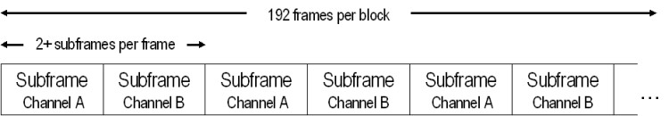
Figure 1: SPDIF block and frame architecture
A single subframe consist of 32-bits: 4 header bits, 4 auxiliary data bits, 20 audio data bits, and 4 status bits. The auxiliary data bits may be combined with the audio data to represent a 24-bit audio sample. The following diagram shows the subframe structure from least to most significant bit.
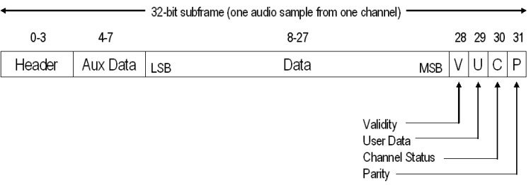
Figure 2: SPDIF subframe architecture
The bits within each subframe are encoded using bi-phase mark coding (BMC). The signal has a transition at the beginning of each bit interval and an additional transition in the middle of the bit interval for an ON bit. An OFF bit has the same signal state for the entire bit interval. The following diagram shows how a set of data bits is encoded into its BMC equivalent using a clock that runs at twice the bit rate.
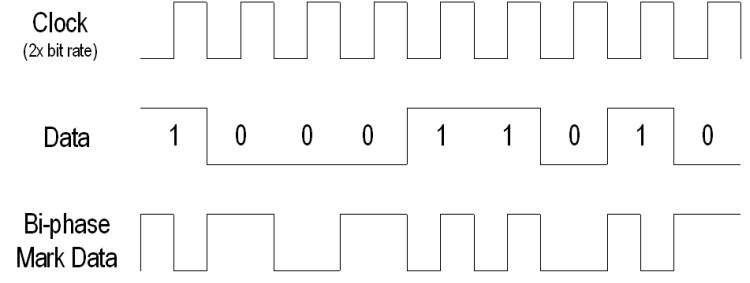
Figure 3: Bi-phase mark coding scheme
The bit rate of the SPDIF data stream is matched to the audio sample rate to create a continuous bit stream without any gaps between subframes, frames, or blocks. For example, a 48 kHz audio sample rate, common in many applications, results in a bit rate of 3.072 MHz and a clock rate of 6.144 MHz. In this case the duration of an OFF bit is ~325.5ns, while an ON bit consists of two alternating ~162.7ns states.
The 4-bit header defined in the subframe structure is used to indicate the start of a subframe and allows the receiver to synchronize itself with the data stream. The structure of the header does not follow the rules of the bi-phase mark coding. It starts with an extra long state (one and half bits in length) which allows the receiver to differentiate the start of the header from the rest of the data stream. There are three different header combinations to indicate the type of subframe that follows. The first subframe in each frame is identified as channel A, while all subsequent subframes are channel B. The first subframe in a new block of frames (192 frames per block) also has a unique header. The following figure illustrates the three different header types.
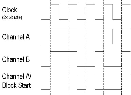
Figure 4: SPDIF header coding
Communication Protocol Implementation
The implementation of a digital communication protocol in LabVIEW FPGA normally consists of two or three diagram components. Each component runs in its own independent loop. Communication and synchronization between independent pieces of the diagram is handled using FIFOs and occurences.
One component of the implementation handles the interface to the physical signal using the digital I/O lines of the RIO device. It reads or updates the digital lines based on a set frequency or based on a separate clock signal or trigger. For a read operation, it returns the most basic piece of information, whether the physical signal is high or low. For a simple protocol, like RS-232, this may represent the actual value of a bit, 0 or 1. Reading 8 bits in sequence at a set frequency (baud rate) returns one byte of data from the serial bus. This basic piece of information is buffered on the FPGA in user memory or in a LabVIEW FPGA FIFO.
In case of simple protocols, this data may already be suitable for transferring to a host application in which case the second component of the LV FPGA VI handles the data transfer from the buffer to the host. For more complex protocols, including SPDIF, we want to process the raw data further into more useful information before passing it to the host application. We will see in the implementation of the SPDIF protocol how it converts the information about individual signal pulses into the 32-bit value contained in a subframe of the protocol. The subframe data is transferred to the host application in a third component on the LV FPGA diagram.
SPDIF in LabVIEW FPGA
Compared to a simple pulse code modulation protocol (e.g. RS-232), SPDIF uses a more advanced coding scheme. The data in SPDIF is not represented by the simple high or low level of the signal. Rather it uses a biphase coding scheme where the data is represented by the length of pulses in the digital signal. Therefore to read SPDIF using the FPGA we need to make repeated measurements of the digital signal and look for changes in the signal to measure the length of the individual pulses on the bus. The pulse lengths become the basic piece of information that we decode to read the SPDIF data.
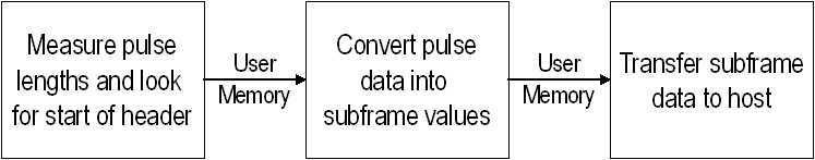
Figure 5: LabVIEW FPGA SPDIF logical diagram
Therefore the first component of our implementation continuously reads the digital input lines and scans for any changes in the signal. Each time the signal changes state it records the length of the completed pulse based on the clock used by the FPGA. In order to synchronize itself with the subframes contained in the FPGA, this component also looks for the extra long start pulse of a subframe and then starts recording the length of all subsequent frames in user memory. Every time it sees the start of a new subframes is sends a message to the second component that the set of pulse lengths for the previous subframe is ready for processing.
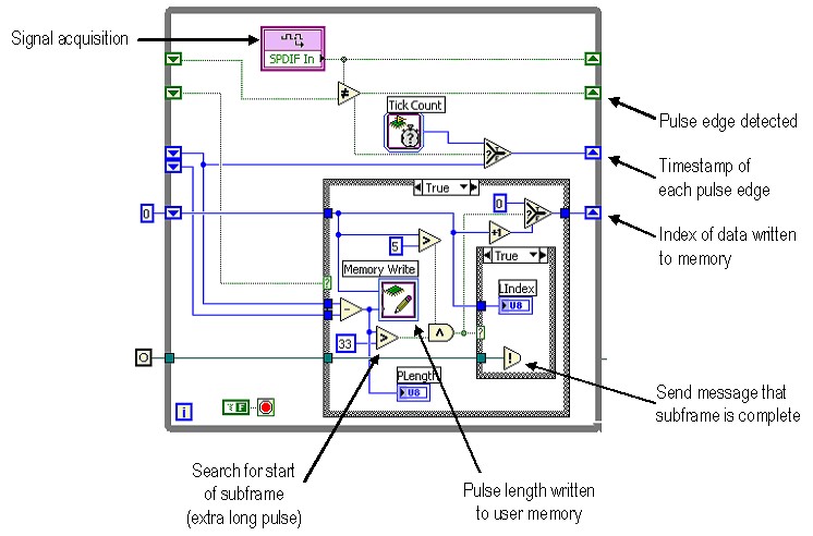
Figure 6: Pulse acquisition on the LabVIEW FPGA diagram
The second component on the diagram retrieves the pulse lengths from the user memory and converts them into the individual bits stored in the subframe. Once it has assembled a 32-bit subframe it stores the value in another portion of the user memory. The header data, which is contained in the first four pulses of each subframe, is stored in the 32-bit word using a custom bit representation since there is no valid interpretation for these bits. The second diagram component also keeps track of the number of subframes received and sends a message to the host application when it has acquired 1024 new subframes.
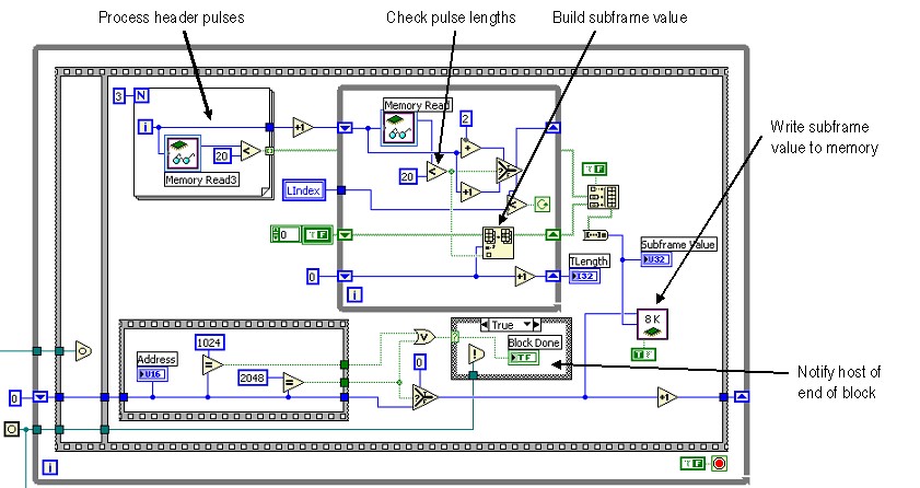
Figure 7: Pulse processing on the LabVIEW FPGA diagram
The host application then uses the third component on the FPGA diagram to efficiently read these 1024 values out of the user memory on the FPGA.
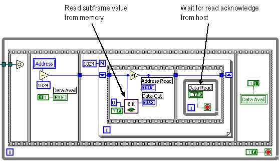
Figure 8: Data transfer to host on the LabVIEW FPGA diagram
While the second component loop is processing pulse lengths and the third component is transferring processed data to the host, the first component continues to measure pulses and store the pulse lengths for processing.
Host Interface
The host interface of the SPDIF input module retrieves subframe data from the FPGA and transfers the data to the host application for display, processing or display. The following figure shows the high level diagram for a monitoring application where data retrieved from the SPDIF signal is split into header, audio, and status data and displayed on different graphs. The SPDIF Read VI retrieves a block of data from the FPGA and returns a two-dimensional array containing the left and right channel data.
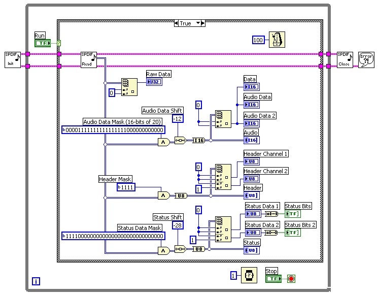
Figure 9: Data display in the LabVIEW host application
The SPDIF ReadVI internally waits for a block of data to be available on the FPGA and then retrieves each of the subframe values in a For loop. After each read operation, it acknowledges the transfer so that the FPGA can retrieve the next value from the buffer. This block-based single line handshaking mode transfers data efficiently from the FPGA to the host application.
After retrieving a block of data the one-dimensional array is resized to separate the left and right channel data and the subVI returns a two dimensional array to the host application.
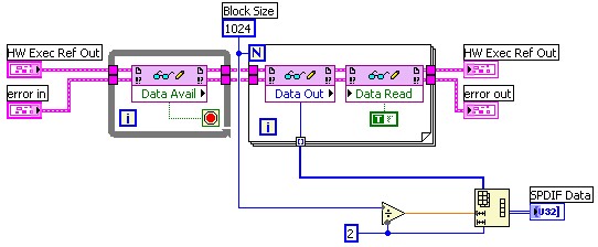
Figure 10: Data transfer in the LabVIEW host interface
Logging SPDIF Data
Instead of displaying the data as it is acquired, the host application may also write the data to a file for later processing and analysis. The easiest and most efficient method is to write the binary data from the FPGA straight into a file as shown in the following figure. A file is opened for binary write mode, and the data, as it comes from the SPDIF Read function, is written into the file. In this case the file does not include any additional information about the number of channels, sample rate, etc. Therefore the application which will read the data file must know the format of the data contained in the file.
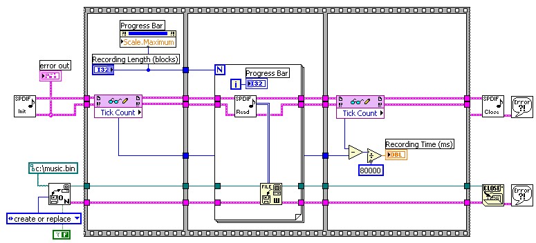
Figure 11: Data logging in the LabVIEW host application
To read the data file written in the previous example use code similar to the following example. The binary data is read as a string from the file and converted into 32-bit integers, representing the subframe values. The one-dimesional array is resized to split the left and right channel data and lastly masked to extract only the upper 16-bits of the analog data (bit 12-27 of the subframe value). The sample rate (48 kHz typical in many applications) is applied to the time axis of the waveform graph displaying the audio data.
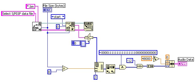
Figure 12: Read data file in the LabVIEW host interface
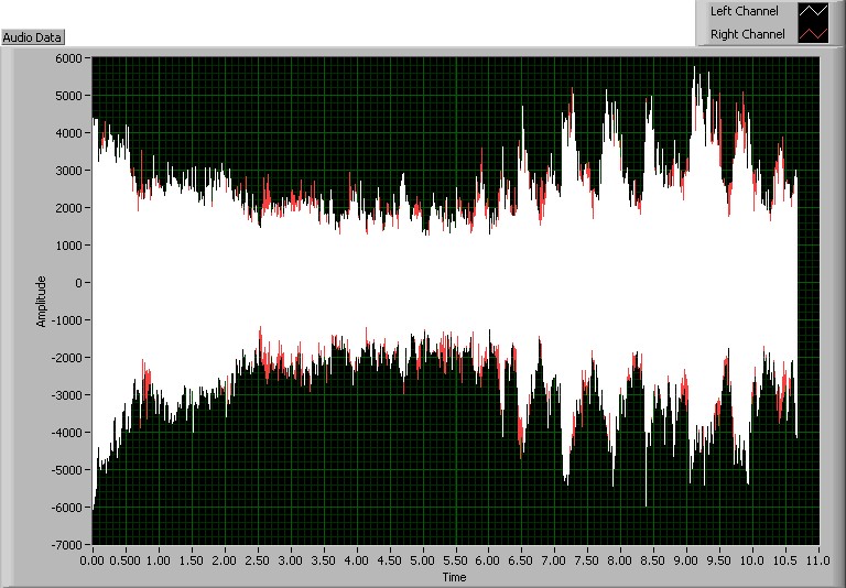
Figure 13: Audio data contained in a sample data file
Other Considerations
Based on the loop rate of the acquisition loop on the FPGA we can calculate the maximum bit rate of the SPDIF data that can be read using this implementation. Because we need to be able to differentiate between the different pulse lengths of the SPDIF data stream, we must oversample the digital signal sufficiently to make this measurement. Based on the implementation shown above compiled with a 80 MHz FPGA clock rate, we can acquire SPDIF data streams up to 48 kHz analog sample rate. To be able to acquire SPDIF streams using 96 or 192 kHz analog sample rates we need to reduce the loop time of the acquisition routine accordingly. This can be accomplished by using the Single Cycle Timed Loop in the LabVIEW FPGA module to improve the performance of the FPGA VI.
As we have seen it is possible to develop a SPDIF input module using the RIO technology and LabVIEW FPGA. However, it currently is not feasible to implement an SPDIF output module without some additional hardware. The FPGA runs at defined clock cycles based on its internal 40/80 MHz clock. The digital lines are read and updated at the same frequency giving us a time resolution of 25 or 12.5 ns for updates and reads. For an input application this resolution is sufficient as we can sample the digital lines faster than the input signal. However, to generate an SPDIF signal we need to be able to update the signal at the intervals defined by the SPDIF standard and the sample rate used. The resolution of the FPGA clock is insufficient for this application and requires an output component that can update a signal at these custom data rates.
Related Links:
S/PDIF Overview