Using a Unity Gain Buffer (Voltage Follower) with a DAQ Device
Overview
Contents
- Introduction
- The Effect of High Source Impedance
- Using a Unity Gain Buffer to Decrease Source Impedance
- Selecting the Proper Components
- Example System Using an OPA2277
- Conclusion
Introduction
Transducers, a common component of any data acquisition system, convert physical phenomena, such as strain or pressure, into electrical signals that can be acquired by a data acquisition (DAQ) device. Common examples of transducers include microphones, thermometers, thermocouples, and strain gauges. When selecting a transducer for use with a DAQ device, it is important to consider the input and output range of the transducer and whether it outputs voltage or current. Often, the sensor and DAQ device require signal conditioning components to be added to the system to acquire a signal from the sensor or to take full advantage of the resolution of the DAQ device. However, the transducer's output impedance is commonly overlooked as a vital consideration when building a DAQ system.
Impedance is a combination of resistance, inductance, and capacitance across the input or output terminals of a circuit. Figure 1 models the resistive output impedance of a transducer and the resistive input impedance of a DAQ device. Realistically, capacitance and inductance are also present in all DAQ systems. It is important that the input impendence of the DAQ device is much higher relative to the output impedance of the selected transducer. In general, the higher the input impedance of the DAQ device the less the measured signal will be disturbed by the DAQ device. It is also important to select a transducer with as low an output impedance as possible to achieve the most accurate analog input (AI) readings by the DAQ device. The following sections address how high output (source) impedance affects a measurement system and how to use a unity gain buffer or voltage follower to decrease the output impedance of a sensor.
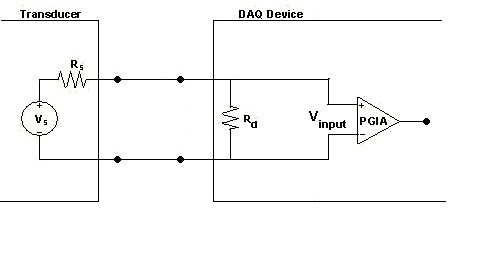
Figure 1. Model of a Typical Transducer and DAQ Device
The Effect of High Source Impedance
If resistive impedances are taken into account, as shown in Figure 1, the output impedance of the transducer and the input impedance of the DAQ device create a voltage divider. The actual input voltage to the Programmable Gain Instrumentation Amplifier (PGIA) in the DAQ device can be calculated by the following voltage divider equation:
Vinput = Vs * ( Rd / (Rs + Rd) )
For example, if Rs and Rd are equal, the voltage seen by the PGIA in the DAQ device is half of the output voltage of the transducer, and this result is not the desired behavior for measurement systems. If Rd is extremely large and Rs extremely small, then Vinput and Vs are almost equal. The desired behavior of the measurement system, this result only takes into consideration the resistive impedances of the transducer and DAQ device. When inductance and capacitance are added to the system, they introduce phase changes and filtering of the signals.
When a multiplexer is used to sample multiple channels, there are other behaviors that must be considered. High source impedance affects a DAQ system by increasing the settling time of the amplifier of the DAQ device amplifier when sampling multiple channels. Settling time is the amount of time that it takes for a measured signal to reach a specified accuracy and to stay within the range tolerance. The settling time increases when sampling high-impedance sources due to the input capacitance of the DAQ device and also due to a phenomenon called charge injection. When the input multiplexer of the DAQ device switches to a given channel, the input capacitance of the DAQ device must be charged through the output impedance of the source. Such output impedance can take a long time if the source impedance is especially high. When a channel is selected in a multiplexer, for example AI channel 0, those capacitors accumulate charge. When the next channel, such as AI channel 1, is selected, the accumulated charge leaks backward through that channel. If the output impedance of the source connected to channel 1 is high enough, the resulting readings can reflect the voltage trends on channel 0, because the injected charge does not decay by the time the signal is sampled. This behavior is commonly referred to as ghosting or crosstalk. In addition, multiplexers contain switches, usually made of switched capacitors. These capacitors dump a small amount of charge into the signal when that channel is selected. If the source impedance is too high, this charge gets trapped between the high output impedance of the source and the high input impedance of the DAQ device and does not decay by the time the signal is sampled. This behavior is referred to as charge injection, a property of all solid-state multiplexers.
As you can see, once a multiplexer has switched to a new channel, two types of error can be built up on the input capacitance of the DAQ device. The first type of error is the residual charge from the previously sampled channel. The second type of error is the charge added to the signal by the multiplexer. For the PGIA to see the correct voltage, all this erroneous charge must dissipate before the signal is sampled. A source with a sufficiently low impedance can quickly dissipate this charge and allows the signal to settle to the correct value before being sampled.
Ideally, source impedances should be kept low (< 1 kW) when sampling multiple AI channels. However, if high source impedance prevents the signal from settling to within the specified accuracy of the DAQ device, you can either reduce the sampling rate to account for the increase in settling time, or you can implement a unity gain buffer (voltage follower) between the transducer and the DAQ device to reduce the impedance of the source.
Using a Unity Gain Buffer to Decrease Source Impedance
When you can neither use a transducer with a low output impedance nor reduce the sampling rate of the DAQ device, you must use a voltage follower that employs operational amplifiers (op-amps) with unity gain (gain = 1) for each high-impedance source before connecting to the DAQ device. This configuration is commonly referred to as a unity gain buffer, and it decreases the impedance of the source connected to the DAQ device. A power supply is required to provide +/- 15 V to the op-amp, and the power supply should be referenced to the analog input ground (AIGND) of the DAQ device.
As shown in Figure 2, the positive lead of the signal is connected to the positive input of the op-amp. The output of the op-amp is then connected to the positive input of the DAQ device, ACH<i>, through a resistor, Ro. Depending on the input channel configuration, the negative lead of the transducer is either connected to another op-amp, as shown in Figure 2, or to AIGND/AISENSE, as shown in Figures 3 and 4. When using floating differential or nonreferenced inputs, a bias resistor must be connected between the negative input and AIGND to keep the signal within common-mode range and to prevent the PGIA from saturating. As shown in Figure 5, a bias resistor, RB, has been connected between the negative signal lead and the COMMON connection of the power supply. For more information on the input channel configuration, refer to Field Wiring and Noise Considerations for Analog Signals.
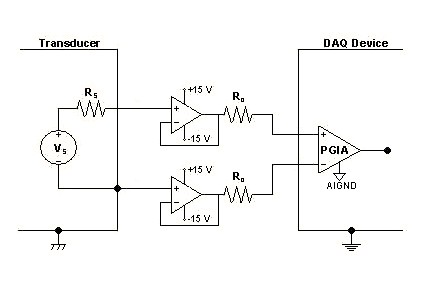
Figure 2. Voltage Follower for Grounded Differential Connections
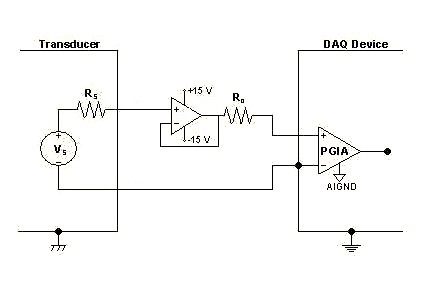
Figure 3. Voltage Follower for Floating Single-Ended Connections
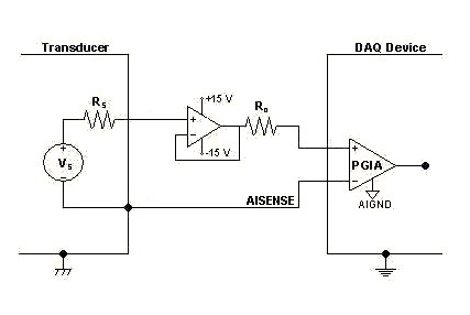
Figure 4. Voltage Follower for Grounded Single-Ended Connections
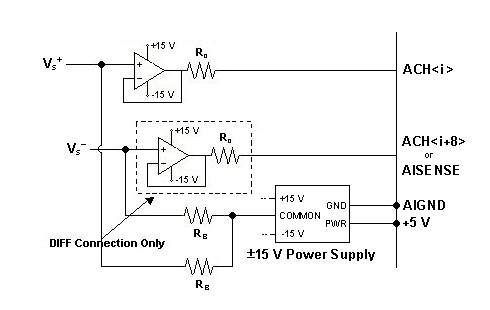
Figure 5. Voltage Follower for Floating Differential or Nonreferenced Connections
Selecting the Proper Components
When adding a unity gain buffer to a measurement system, it is important to select the proper components to maintain measurement accuracy and performance. Important considerations for selecting the op-amp include:
- +/- 15 V (> 32 V process) clean power supply referenced to AIGND
- Use a precision, low-noise op-amp with FET inputs for optimal performance
- (Recommended) RsIB < 1 LSB for desired gain
- Rs = Source impedance
- IB = Op-amp bias current
- The RMS noise added by the new circuitry should be less than the RMS noise of the DAQ device.
Where:e n = Op-Amp Input Voltage Noise Density
i n = Op-Amp Input Current Noise Density
f = Device Input Bandwidth (Hz)
- Offset Voltage Drift < 1 LSB/oC
Additional considerations include:
- (Optional) Ro = 50 Ω; Ro must be large enough to keep op-amp stable when connected to a capacitive load like a cable.
- (Optional) A capacitor can be placed between the positive and negative leads of the source to limit resistance noise from the source impedance.
NOTE: These recommendations are suggestions, not rules. Your error budget ultimately determines the requirements for the op-amp that you select.
Example System Using an OPA2277
When a Burr-Brown OPA2277 op-amp is used with a NI 6052E and a sensor with a 1 MW source impedance, the NI 6052E acquires data at a gain of 0.5, which provides an input range of -10 to +10 V. Using these settings, 1 LSB is equivalent to 305 mV.
Determine the added noise by calculating :Where:

The new system noise can now be calculated. Note that the added op-amp noise must be counted twice for a differential measurement. Where:
The increased system noise due to the addition of the unity gain buffer to the system can be compensated for by increasing the number of points that you average when making a DC measurement. Averaging improves the relative accuracy of measurements.
Calculate the new system DC specifications:
Calculate RsIB:
For this configuration, the bias offset voltage is over 6 LSBs. However, the offset voltage drift for this op-amp is +/- 0.25 mV/oC which means that DC offset error can be calibrated out of the system if the system temperature remains relatively constant. Calculate the Unity Gain Offset Error (UGOE). Be sure to multiply RsIB by 2 for a differential measurement, if needed:
Where Vos = Op-Amp Input Offset Voltage = 25 mV.
To determine the new absolute accuracy of the system, the UGOE must be added to the absolute accuracy of the NI 6052E. Absolute accuracy is the specification that you use to determine the overall maximum error of the measurement. The absolute accuracy of the NI 6052E at +/- 10V is 4.747 mV.
Depending on the individual system requirements, the increased amount of error may or may not be acceptable for the measurement system.
Conclusion
When scanning multiple channels at high sampling rates, be careful to notice the settling time and the impedance of the source of each channel. If the source impedance is too high, charges that accumulate on the input capacitance of the DAQ device are not dissipated by the time the signal is sampled. The result of this behavior is that the signal often appears to follow the signal of the previous channel. In this situation, either the sampling rate or the source impedance must be decreased. If the sampling rate cannot be decreased, the source impedance of the signal can be decreased by using a unity gain buffer or voltage follower. When adding a voltage follower to the measurement system, be mindful of the allowable measurement error and accuracy when selecting components and the input configuration for the DAQ device. However, keep source impedances below 1 kW when sampling multiple channels whenever possible.