NI SourceAdapt Next-Generation SMU Technology
Overview
Source measure units (SMUs) are an important class of instruments used for testing the current-voltage (I-V) characteristics of a wide range of devices, from electronic components such as transistors to integrated electronic products such as portable music players or medical devices. NI SourceAdapt technology from NI, featured for the first time on the 4-channel NI PXIe-414x precision SMUs, is a next-generation technology powered by a digital control loop instead of the traditional analog control loop. With NI SourceAdapt technology, you can customize the response to any load, so you can achieve an ideal response with minimum rise times and no overshoots or oscillations. NI SourceAdapt is now featured on all NI Precision System SMUs, as well as the PXI Electronic Load Module and select options of the PXI Programmable Power Supply. Let’s take a behind-the-scenes look at SourceAdapt technology. This article will primarily discuss SourceAdapt operation as it relates to an SMU, but it works in the same way for a PXI Electronic Load Module or a PXI programmable Power Supply.
Contents
- Introduction
- Limitations of Traditional Analog Control Loops
- Understanding the Architecture Behind SourceAdapt Technology
- Working With Reactive Loads
- Using the Feedback Compensator
- Achieving Ideal Response with Your SMU
- Conclusion
- Next Steps
Introduction
SMUs use closed-loop feedback control to ensure that the programmed source value (setpoint) is correctly applied to the load under test. Traditional SMUs have used analog hardware to implement the control loop, but this comes with trade-offs. For example, a high-bandwidth SMU designed for high-speed testing is typically not suitable for testing highly capacitive loads that require high stability. On the other hand, an SMU designed to test high-capacitive loads is not likely to be the best option for high-speed testing. In fact, most traditional SMUs are optimized for either high-speed or high-stability test. Even then, it is difficult to achieve an optimal response because it is extremely difficult to design circuitry that provides just the right response for a range of loads.
NI SourceAdapt technology fundamentally addresses this issue by helping you custom-tune the SMU response to a given load. This provides an optimal SMU response with minimal settling times, which leads to shorter wait times and faster test times, and it eliminates overshoots to protect the device under test (DUT) and oscillations to ensure system stability.
Because tuning the SMU response is done programmatically, an SMU configured for a high-speed test can be easily reconfigured for a high-stability test – maximizing the return on investment of the test equipment and achieving better results.
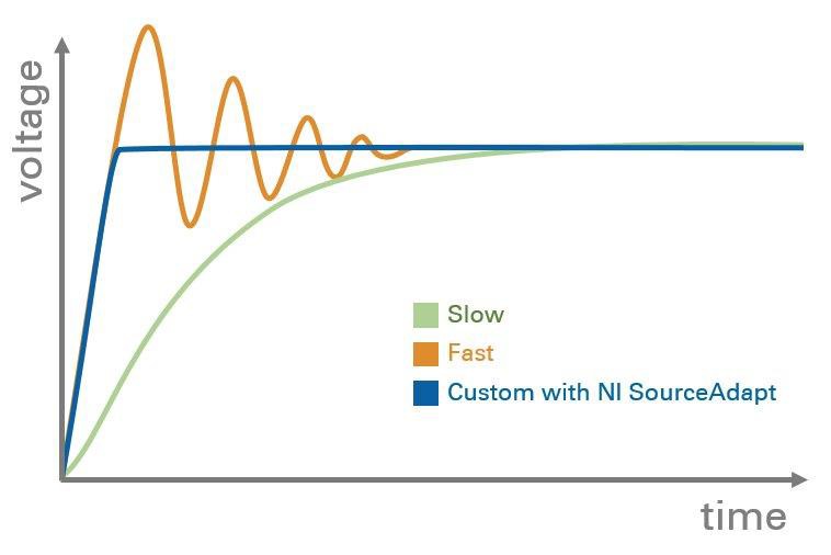
Figure 1. SMU Response to a Capacitive Load. NI SourceAdapt technology enables customized response (red) for maximum stability and minimum transient response times.
Limitations of Traditional Analog Control Loops
In the past, test instrument vendors have taken different approaches to providing a configurable transfer function. They have traditionally involved switching reactive elements in and out of the control loop’s feedback path, an approach that is limited in its effect, configurability, and extensibility. Truly custom compensation, to the degree afforded by SourceAdapt technology, required completely rethinking how the SMU control loop is architected.
The control loop of an SMU is a superposition of two closed control loops: one for current and one for voltage. Figure 2a shows a conceptual view of a traditional SMU architecture.
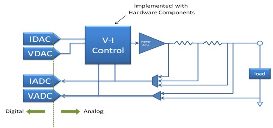
Figure 2a. Simplified View of a Traditional SMU Architecture. Note that the control loop (the V-I Control) is implemented using analog hardware components, thus providing very limited configurability.
The V-I Control is given setpoints for voltage and current, and its closed-loop feedback allows it to precisely control the output voltage and current to match those setpoints. This entire control loop is implemented using amplifiers and other active analog hardware. The feedback signals are also read by analog-to-digital converters (ADCs) to provide high-precision measurements. Varying the compensation for this architecture requires the addition of discrete reactive components. To a degree, you can make such adjustments programmatically by using switches, but this is a limiting and insufficient approach. At most, it allows you to choose one of a small number of possible configurations. This falls short of optimizing the SMU response to a given load. So, how can you achieve an arbitrarily configurable control loop? The answer to this lies in a brand new architecture as shown in Figure 2b.
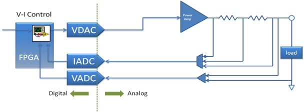
Figure 2b. The New NI SMU Architecture. Note that the control loop (the V-I Control) has moved to the digital domain inside a field-programmable gate array (FPGA).
In this new architecture, the V-I Control has been moved into the digital domain, and now resides within an FPGA. A digital control loop, unlike an analog one, is completely software configurable to optimize the control loop for achieving an ideal response for the load at hand. This particularly versatile implementation of the control loop makes SourceAdapt technology possible – providing the ability to customize the SMU response to any load.
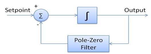
Figure 3. The New Digital V-I Control Implementation
The V-I Control contains an integrator that provides DC accuracy and the general regulation for the loop, and a pole-zero Filter, which enables custom compensation. Both of these blocks are user configurable to an extent that’s simply not possible with an analog control loop. And, by leveraging fast ADCs and DACs, as well as harnessing the processing power of FPGAs, the overall loop is perfectly capable of handling precision source measure applications. The result is a very configurable architecture that does not compromise on performance.
Understanding the Architecture Behind SourceAdapt Technology
The new architecture featured in SourceAdapt technology allows transfer function adjustments in two ways. First, you can adjust the gain-bandwidth product (GBW) on the integrator, and, second, you can use the feedback compensator as either a lead or a lag compensator, which allows the user to add a pole-zero pair at an arbitrary frequency in the transfer function.
Gain-Bandwidth Adjustment
The integrator on the output path provides an open-loop transfer function that looks similar to that of an operational amplifier on the Bode magnitude (gain margin[1]) and phase margin[2] plots.
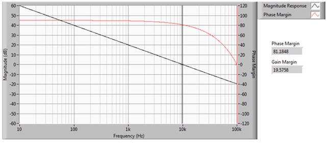
Figure 4a. Open-Loop Transfer Function of the Integrator (Gain Margin: Left, Phase Margin: Right)
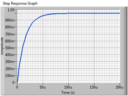
Figure 4b. Corresponding 1 V Step Response With Unloaded Output (for the Transfer Function in Figure 4a)
By adjusting the integrator gain, or the GBW of the loop, you can adjust the overall response of the loop to behave
- Slower and more stable, for example, with a GBW of 3 kHz and phase margin of 87.34 (see figures 5a and 5b)
- Faster, for example, with a GBW of 20 kHz (see figures 6a and 6b)
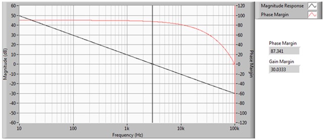
Figure 5a. Slower, More Stable Response With 3 kHz GBW and a Phase Margin of 87.34
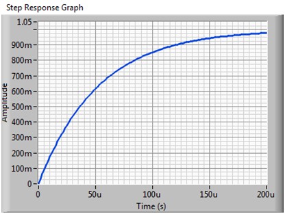
Figure 5b. Corresponding 1 V Step Response With Unloaded Output (for the Transfer Function in Figure 5a)
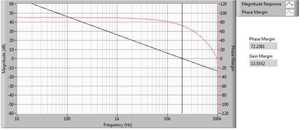
Figure 6a. Faster Response With 20 kHz GBW and a Phase Margin of 72.23
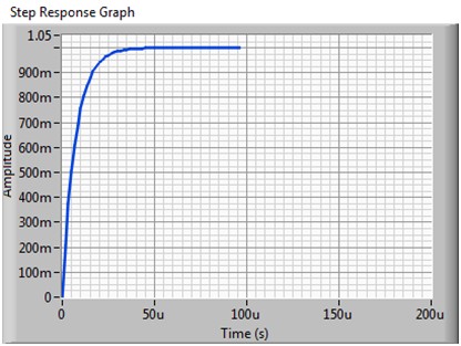
Figure 6b. Corresponding 1 volt Step Response with unloaded output (for the Transfer Function in Figure 6a)
Working With Reactive Loads
You can force more challenging reactive loads that tend to be less stable to behave in a more stable fashion simply by slowing down the loop. Figures 7a and 7b demonstrate the behavior of the control loop with a capacitor as a load. A capacitor introduces a pole at a frequency inversely proportional to the capacitance and the output stage’s shunt resistor, affecting both gain and phase. The resulting open-loop frequency response for a 0.1 µF capacitor is shown in Figure 7a with accompanying step response in Figure 7b.
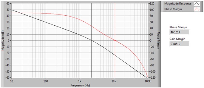
Figure 7a. The open-loop transfer function is marginally stable with 0.1 µF capacitor as a load.
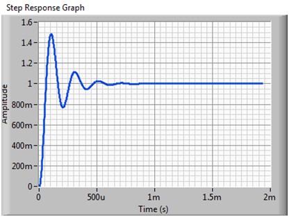
Figure 7b. Corresponding 1 V Step Response With 0.1 µF Capacitor as a Load
As shown in Figure 7b, the response is under-damped; it overshoots and takes a long time to settle. Adjusting the GBW makes this system behave better. If the primary concern is to eliminate the overshoot completely, then you can slow down the loop enough to get the response without any overshoot. Figures 8a and 8b show a slowed-down response with a 500 Hz GBW to completely eliminate the overshoot.
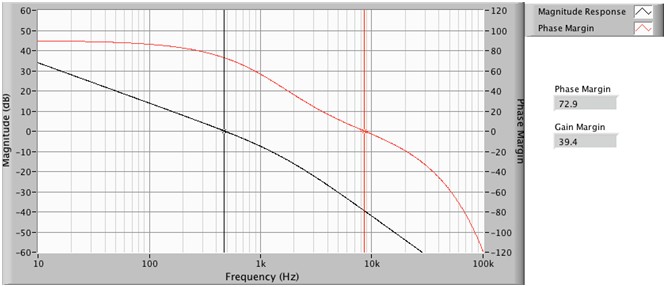
Figure 8a. Open-Loop Transfer Function With 500 Hz GBW (Load: 0.1 µF Capacitor)
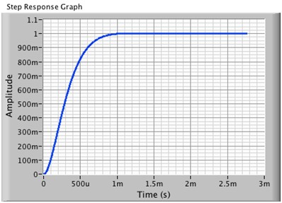
Figure 8b. Corresponding 1 V Step Response with 500 Hz GBW (Rise Time ~1 ms)
Although the overshoot is eliminated, the response of the system is now very slow. To achieve an optimal response – the second method of adjusting the transfer function, the feedback compensator (as a lead or a leg compensator) can be used.
Using the Feedback Compensator
SourceAdapt technology provides the second tool to optimize the response: the feedback compensator. Continuing with the example from the previous section, the goal is to achieve a fast rise time while avoiding overshoots and oscillations. This is accomplished by using a compensator to counteract the pole introduced by the capacitor. With such control, it is permissible to further increase the GBW to achieve a faster rise time while remaining very stable. Increasing the GBW to 20 kHz, Figure 9a shows a comparison between the magnitude and phase response using a compensator versus not using one.
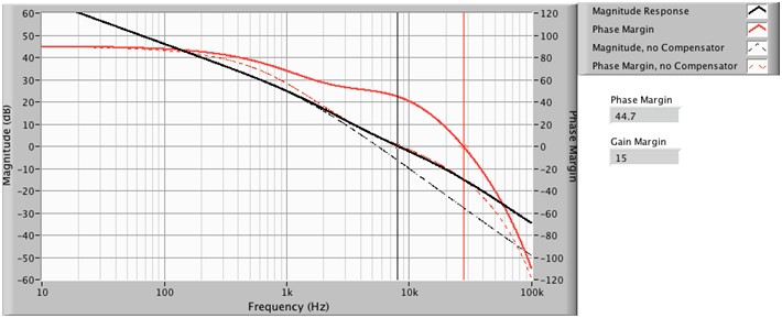
Figure 9a. Open-Loop Transfer Function With and Without the Compensator (GBW: 20 kHz, Load: 0.1 µF Capacitor)

Figure 9b. Corresponding 1 V Step Response With 20 kHz GBW and Compensator (Rise Time ~100 µs)
As shown in Figure 9b, the response is ideal with a 10X reduction in rise time, no overshoot, and excellent stability with a phase margin around 45 degrees.
Achieving Ideal Response with Your SMU
Because your load directly affects the transfer function of the source measure unit (SMU) control loop, achieving ideal response requires configurability for a given load. With NI SourceAdapt technology, you can customize the SMU response to any load, so you can achieve an ideal response with minimum rise times and no overshoots or oscillations. This means you can implement tests faster without the risk of potential device under test damage or system stability issues.
Conclusion
This article describes the need to be able to configure an SMU transfer function to provide ideal responses to various loads and how you can achieve complete configurability with new NI SourceAdapt technology. With SourceAdapt technology, you can now completely customize SMU response to any load to generate an ideal response with minimum rise times, no overshoots, and no oscillations. You can test DUTs faster without the risk of accidental damage or system stability issues.
SourceAdapt technology is made possible by the latest advancements in NI LabVIEW embedded technology, which extends the LabVIEW graphical development environment to FPGAs.
[1] The gain margin is defined as the change in open-loop gain that is required to make the system unstable.
[2] The phase margin is defined as the change in open-loop phase shift required to make a closed-loop system unstable.