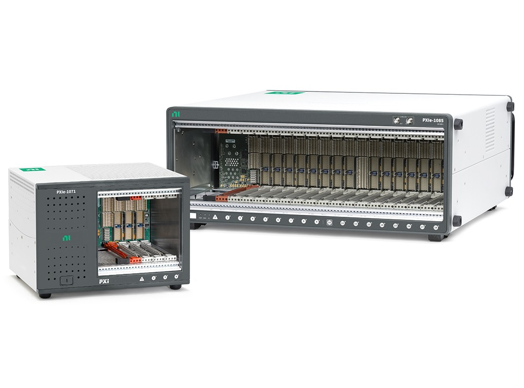
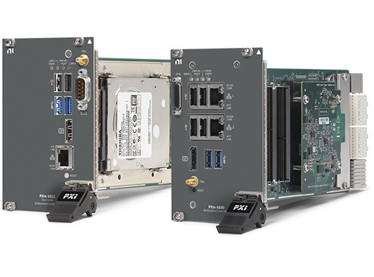
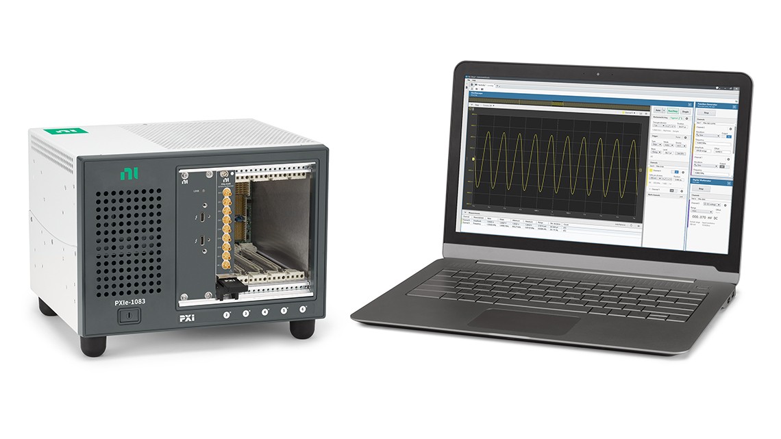
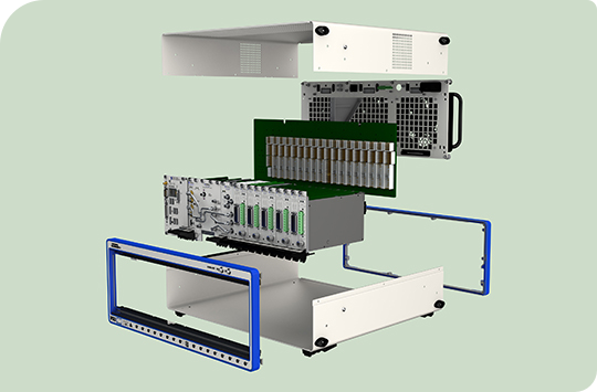
From 01:00 AM CDT Saturday, June 10 - 04:00 AM CDT Saturday, June 10, ni.com will undergo system upgrades that may result in temporary service interruption.
We appreciate your patience as we improve our online experience.
From 01:00 AM CDT Saturday, June 10 - 04:00 AM CDT Saturday, June 10, ni.com will undergo system upgrades that may result in temporary service interruption.
We appreciate your patience as we improve our online experience.
Today’s latest electronic designs are characterized by their converging functionality and the increasing prevalence of seemingly interwoven analog and digital technology. Designing, prototyping, and testing these systems, such as 3G wireless handsets and set-top boxes, where video, audio, and data are converging, requires tightly integrated digital and analog acquisition and generation hardware matched in base-band sampling rate, distortion, and timing characteristics. Analog and digital instrumentation can no longer be stand-alone systems with disparate timing engines and mismatched analog performance. Furthermore, with manufacturing of such devices running around the clock in many locations around the world, the need for stability and consistency of performance specifications over a wide temperature range is compulsory for reliable, high-throughput functional test.
National Instruments designed the Synchronization and Memory Core (SMC) as the common architecture for a suite of high-speed modular instruments that answer the challenge of testing converged devices. The important SMC features that are critical to integrated mixed-signal prototyping and test systems are:
1. Flexible input and output data transfer cores
2. High-speed deep onboard memory scalable up to 256 MB per channel
3. Precise timing and synchronization engine
Three instruments that are matched in both sampling rate and flexibility to form a SMC-based mixed-signal test suite are:
Central to the SMC architecture is a field-programmable gate array (FPGA) controller, the DataStream FPGA (DSF), which is the "CPU" of the instrument. It processes all instructions, listens to triggers and locks, routes signals externally, and manages waveform traffic between the instrument and the host computer.
Two major data transfer cores are instantiated in the DSF: one for input and one for output. The input core is designed for high-speed analog waveform digitization and digital waveform input. The output core is designed for high-speed analog waveform generation and digital waveform output. The data transfer cores in the DSF handle data and instruction processing, event triggering, trigger and marker routing, waveform buffer linking and looping, and interdevice and intradevice communication buses (Figure 1).
The memory subsystem is composed of two blocks, each of which can be separately configured as an input or an output bank. This configuration provides for a 2-channel input device, such as a high-speed 2-channel digitizer, to use both memory banks for data capture. A single-channel arbitrary waveform generator includes a single memory block, configured for output, and a digital waveform generator/analyzer can use one bank for input and the other for output.
Each memory block can be as large as 256 MB, allowing a total of 512 MB per instrument. The port to each memory block is a 64-bit 133 MHz bus with a sustained throughput of more than 1 Gbytes/s per memory block. The memory subsystem is connected through the NI-MITE ASIC to the PCI bus at full bandwidth for fast download or upload of waveforms between the host computer and the SMC.
Figures 2, 3, and 4 show the details of the high-resolution digitizer, the arbitrary waveform generator, and the digital waveform/analyzer daughter cards.
The DSF input transfer core handles high-speed data input streams, whether from digital waveform inputs of a digital waveform generator/analyzer or the analog-to-digital converter (ADC) of a high-speed digitizer. Multiple independent acquisitions can be captured into individual records, ranging from a single buffer to more than two million smaller records, with a rapid 2 µs re-arm time between records. The deep memory easily handles the large data records often required in communications test systems for capture of packet transactions, measurement of clock jitter, and other error diagnostic tests. Thanks to the free-running counters in the DSF timing and synchronization engine, all records can be correlated in time back to their original source. For example, with an external trigger arm signal, the DSF can timestamp all acquired records to the trigger arm signal with 10 ns resolution. On the NI 5122 digitizer, the timestamping resolution can extend down to 100 ps with time-to-digital conversion (TDC) technology. With deep memory, multiple record segmentation, 100 ps timestamping resolution, and fast re-arm time, you can capture rare, sporadic, or rapidly occurring events while still maintaining high sample rates. This feature increases the effective memory size by acquiring only regions of interest without losing time coherence between the captured waveforms.
For output devices, such as the NI 5421 arbitrary waveform generator and NI 6552 digital waveform generator/analyzer, the sequencing instructions are stored in the same physical memory as the waveforms. Traditional arbitrary waveform generators are based on architectures where instructions for sequencing waveforms are stored in physically separate SRAM memory comprised of a few kilobytes, which severely limits the maximum number of waveforms that can be sequenced. The SMC takes a unique, far-more-flexible approach by combining the instructions along with waveforms in the same physical memory so that you are not constrained by a very limited number of sequencing instructions. With memory configurations ranging up 256 MB, you have the flexibility to use as much memory as you need for sequencing instructions. A closer look at the arbitrary waveform generator sequencing specifications sheds some light on the flexibility of shared memory between waveforms and instructions as seen in the following tables.
A traditional arbitrary waveform generator (AWG) may feature the specifications for waveform memory and sequencing capabilities shown in Table 1.
The specifications shown in Table 1 are fixed for the traditional AWG. It cannot exceed 4,096 steps for a given sequence. The NI 5421 arbitrary waveform generator, with the standard memory of 8 MB, offers the flexible waveform memory and sequencing capabilities shown in Tables 2, 3, and 4 because of its shared memory format.
The scenarios shown in the previous tables are representative of what is achievable with shared waveform and instruction memory. With shared memory, you can use the memory space for very long sequences with small waveforms, short sequences with very large waveforms, or a balance in between. Furthermore, with the 32 MB and 256 MB deep memory options, the maximum sequencing specifications increase as well as the waveform memory. Deeper memory on traditional AWGs increases only the waveform memory and does not allow more sequence steps or waveform segments. Deep waveform memory can handle very long waveforms, but in some cases, deep waveform memory alone may not address very demanding applications. A complex sequence of segments defining a waveform can reduce the memory requirements of such applications.
For example, a video frame(s) contains many repetitive segments, such as vertical and horizontal sync pulses, the color burst, and blanking lines in the vertical blanking interval. With the SMC output data transfer core, a copy of each signal segment can be stored, and instructions (on linking and looping the sections) are stored in a sequence. In such an application, the large memory buffer may not be adequate for storing the entire image or multiple images, but can be accommodated by storing the key sections of the image and the sequence list specifying the generation of the frame(s). Such a sequence could easily consume more than the few kilobytes of SRAM instruction memory available in traditional AWGs. With the SMC architecture, the problem disappears with the large memory configurations where you can store the relevant segments of the frames(s) and the large sequence(s).
The SMC output engine optimizes test throughput because you can store multiple sequences, as shown in Table 5, thereby eliminating the setup time between tests. This feature, coupled with deep memory, can significantly increase test throughput because you can switch quickly from one sequence to another within a functional test that requires different test sequences. This capability is especially important for video testing where a set of industry-standard test patterns needs to be generated in rapid succession.
A key requirement in many applications, ranging from video to communications, is large waveform generation and acquisition. Video test image generation with AWGs, sparkle code test of ADCs with digital waveform generators/analyzers, and error vector magnitude (EVM) measurements of baseband modulators/demodulators with digitizers are some of the myriad of applications requiring deep memory for waveform capture and generation.
The SMC input and output data transfer cores are designed to arbitrate waveform movements between the memory banks and the front-end electronics of the instrument at 100 MHz. Incorporated into the SMC, along with the DSF, is the National Instruments SCARAB memory controller, which provides the interface between the memory banks, the DSF, and the National Instruments MITE, a scatter-gather DMA controller. The SCARAB effectively keeps track of where waveforms and instructions are stored in memory and fetches the appropriate data upon request from the DSF and the MITE. It also provides the capability to stream waveforms to and from the memory at the full sampling rates at a sustained pace to accommodate large waveform acquisition and generation. The SMC input core treats the deep memory as a 2-port FIFO buffer, whereby it moves the data at the full sampling rate of 100 MHz from the ADC of the digitizer or the digital lines of the digital waveform generator/analyzer into the memory banks and streams data to the host PC at the available bandwidth of the PCI bus.
The SMC output core treats the memory in a relatively more complex manner because of the shared data and instruction format of the memory. It has to stream data to the digital-to-analog converter (DAC) of the AWG or the digital lines of the digital waveform generator/analyzer at the full sampling rate of 100 MHz, meanwhile extracting the instructions for sequencing the output waveforms at a rate whereby the full sampling rate of 100 MHz is guaranteed. Because of potentially large sequences ranging into hundreds of thousands of instructions, it is not possible to compile all of the sequencing instructions in the DSF at the start of generation due to FPGA size constraints. Therefore, the SCARAB has not only to pull out waveforms from the deep memory at the full sampling rate of 100 MHz but also to provide the sequence instructions to the DSF to execute in real time.
Synchronization is key for either synchronizing instruments of the same type (homogeneous synchronization) for channel expansion, or for tightly correlating the input and/or output of two different instruments (heterogeneous synchronization). By definition, mixed-signal test systems require the use of at least two of the three instruments (digitizer, arbitrary waveform generator, and digital waveform generator/analyzer), as shown in Figure 5. Additional applications requiring synchronization are baseband I/Q signal generation and acquisition for communications, RGB video signal generation and acquisition for consumer electronics, digital waveform generation and acquisition of 24 channels for 24-bit ADC and DAC test, and many more.
The goal of synchronization is to be able to generate and receive waveforms precisely among multiple SMC instruments. In the case of two arbitrary waveform generators, for example, this goal demands that two AWGs generate identical waveforms in perfect alignment with the ability to skew the phase between the waveforms. With sampling rates of 100 MHz on all three devices, proper care and attention was given to the clock and trigger distribution between all devices. Sample clock skew adjustment with tens of picoseconds resolution, trigger propagation delay and skew calibration, and picosecond level rms clock jitter on all devices deliver the performance required to integrate all three devices at 100 MS/s at the subnanosecond level.
Synchronization is implemented by sharing triggers and reference clock between multiple devices. The reference clock can be supplied by the designated master device or by a dedicated high-precision clock source. Each SMC instrument has voltage-controlled crystal oscillators (VCXOs) phase-locked to the PXI 10 MHz reference clock, as shown in Figure 6. To achieve further timing accuracy, you can consider equipment such as rubidium or oven-controlled crystal oscillator (OCXO) based frequency sources. The accuracy of these devices can be better than ±100 parts per billion (ppb). For example, an OCXO source with ±100 ppb accuracy yields a 10 MHz clock with ±1 Hz uncertainty. The NI PXI-6653 Slot 2 timing and synchronization controller is ideal for such applications. It can drive its OCXO clock onto the PXI 10 MHz reference clock lines instead of the PXI backplane clock. Thus, all instruments with VCXOs locked to the 10 MHz OCXO inherit the ±100 ppb accuracy.
Mixed-signal test requires instruments running at different sampling rates to be synchronized, and data must be sampled on the correct sample clock edge on each instrument. When sample clocks on different instruments are integer multiples of the 10 MHz reference clock, all instruments have sample clocks that are synchronous to each other; the rising edge of all sample clocks is coincident with the 10 MHz clock edge. When sample clocks are not integer multiples, such as 25 MHz, there is no guarantee that the sample clocks are in phase, despite being phase-locked to the 10 MHz reference clock (Figure 7). A standard technique to solve this problem is to reset all of the phase-locked loops (PLLs) at the same time, leading to sample clocks of the same frequency that are in-phase (Figure 8). Even though all sample clocks are in phase at this point, the solution is still not complete. Perfect synchronization implies the data clocked from device to device corresponds to within a sample clock cycle. To do this, a trigger must be passed from the master device to the slave device, indicating the beginning of the acquisition or generation. The key to perfect synchronization is the combination of sample clock alignment with triggering.
The distribution of the trigger signal across multiple devices requires passing a trigger signal into the clock domain of the sample clock so that the trigger is seen at the right instance in time on each device. With sample clock rates at 100 MS/s, trigger propagation delay and slot-to-slot skew become major obstacles to accurate trigger distribution. Another distribution channel is needed; the trigger signal needs to be distributed reliably through a slower clock domain and then transferred back to the high-speed sample clock domain of the receiving instrument. A logical choice is to synchronize the trigger signal distribution with the 10 MHz reference clock. However, this configuration still cannot ensure that two boards see the trigger assertion in the same sample clock cycle. To illustrate this point, assume two boards have the simple circuit shown in Figure 9 for trigger transfer from the 10 MHz reference clock domain to the sample clock domain.
Even if the sample clocks of the boards are aligned, the timing diagram in Figure 10 shows why the trigger may not be seen in the same sample clock cycle on both devices.
The output of the first flip-flop (cTrig) may occur too close to the rising edge of the sample clock, causing mTrig to be metastable. When the metastability finally settles, it may do so differently on two different devices, causing them to see the same trigger signal at two different instants in time.
The SMC employs a unique patent-pending digital synchronization scheme whereby another clock domain signal is used to enable the driving and receiving of triggers. This signal, called the Trigger Clock (TClk), is generated by dividing the sample clock down to a frequency low enough that triggers can be reliably transmitted and received over the PXI trigger lines or Real Time System Integration (RTSI) bus. This technique ensures synchronization among supported instruments, independent of the relationship of the sample clock to the 10 MHz reference clock.
Although it is not a part of SMC itself, the driver software that interfaces with the SMC is an important component in realizing the benefits of flexible data cores, deep onboard memory, and the timing and synchronization engine. To interface with the SMC, National Instruments developed a common driver foundation based on the new NI-DAQmx architecture to enable a higher level of integration and operational efficiency. Clocking, memory control, signal routing, PCI bus interfacing, and other functional aspects are unified in software for a matched set of features across product lines.
NI-HSDIO for digital waveform generators/analyzers, NI-SCOPE for High-Speed digitizers, and NI-FGEN for signal generators are three of the instrument drivers built on the NI-DAQmx architecture. These drivers are optimized for high measurement throughput by improving on many aspects such as faster DMA transfer of waveforms over the PCI bus and multithreaded architecture for parallel operation with minimal operating system kernel transitions.
One of the key requirements that drove development of the SMC architecture was high measurement throughput. Manufacturing test and design validation and verification are two areas that demand continuously increasing test throughput. The SMC uses the NI MITE, an ASIC developed to address data transfer over the PCI bus. Unlike many commercial off-the-shelf PCI bus mastering solutions, where only quick burst transfer is available, the MITE is optimized for burst as well as continuous data transfer. Using the NI-DAQmx architecture, the SMC-based instruments improve on past performance to deliver 10 to 17 percent increases in waveform transfers. Figure 11 shows the performance improvements due to the improved software architecture and optimized hardware. The graph shows three standard pulse measurements. The NI 5122 measurements are the fastest, ranging from 47 to 210 times faster than GPIB-controlled oscilloscopes, and you can see that the improvements in software show a slight, but tangible, improvement in measurement speed over past National Instruments digitizers.
By providing a common architecture for the 100 MS/s mixed-signal test suite of instruments, the SMC enables the instruments to test systems where digital and analog signals are side by side. Emphasis on tight timing and synchronization, deep and flexible onboard memory, and fully programmable data transfer cores, makes the SMC an excellent foundation for a mixed-signal modular instrumentation test platform for today and the future.