Synchronous Communications and Timing Configurations in Digital Devices
Overview
High-speed digital input and output communications require tight synchronization and timing parameters for reliable data transmission. The different considerations for timing of a digital signal and the different modes of communication and synchronization are discussed in this document.
Contents
- Introductions to Voltage Definitions
- Timing and Digital Data transfer
- Synchronous Transfer
- Asynchronous transfer
- Data Delay
- Jitter and Noise
- The Real Picture
Introductions to Voltage Definitions
In single-ended signals, a digital transmitter drives out one voltage (called VOL or Voltage Output Low) to represent a logic level ‘0’ and another voltage (called VOH or Voltage Output High) to represent a logic level ‘1’. Both of the VOH and VOL voltages are referenced to ground. At the single-ended digital receiver any voltage less than one voltage (called VIL or Voltage Input Low) is interpreted to represent a logic level ‘0’, and any voltage greater than a voltage (called VIH or Voltage Input High) is interpreted to represent a logic level ‘1’.
TTL (Transistor – Transistor Logic) logic is a single-ended signal, where VOL is equal to ground and VOH is commonly 3.3V or 5V. The difference between VOH and VIH and the difference between VOL and VIL is the NIM (Noise Immunity Margin). The NIM determines how much noise can be on the digital signal before the receiver cannot correctly receive the digital signal.
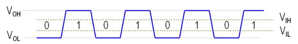
Figure 1 – Single Ended Signal
Differential Signals take two wires configured as a pair, instead of 1 wire and a ground to transmit digital signals. Differential signals have one distinct advantage: they are immune not most types of signal noise. The receiver interprets the signals based on the voltage difference between the pair of signal – not based on a reference to ground. For the differential digital signal to be received as a logical ‘0’, the V+ signal must be less than the V- signal by more than Vdiff.

Figure 2 – Differential Signal
The digital driver still drives out two voltages, VOH and VOL as in the single-ended case. This Vdiff is specified by the particular voltage standard. For example, the Vdiff for LVDS is 100mV. While differential signals are not specifically referenced to ground like single-ended signals, they are generally limited in the range of valid voltages. This is usually specific in terms of the midpoint or average of the two voltage levels and is called the common mode voltage (VCM).
Some kinds of differential signals are LVDS (Low Voltage Differential Signal), ECL (Emitter Coupled Logic), PECL (Positive Emitter Coupled Logic) and RS-422.
LVDS transmits two different voltages which are compared at the receiver. LVDS uses this difference in voltage between the two wires to encode the information. The transmitter injects a small current, nominally 3.5 mA, into one wire or the other, depending on the logic level to be sent. The current passes through a resistor of about 100 to 120 Ω (matched to the characteristic impedance of the cable) at the receiving end, and then returns in the opposite direction along the other wire. From Ohm's law, the voltage difference across the resistor is therefore about 350 mV. The receiver senses the polarity of this voltage to determine the logic level. This type of signaling is called a current loop.
Also see: Interfacing to LVDS with the NI 655X Digital Waveform Generator/Analyzer
Timing and Digital Data transfer
Understanding when to sample and when to generate is crucial for data transfer. If you violate some kind of timing information you could risk sampling the data twice or missing a sample. You could also sample during the transition of the data lines, which would cause erroneous data to be transmitted or generated.
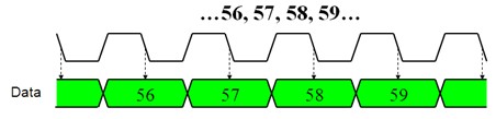
Figure 3 – Timing of Digital Data
In the diagram below, since the timing is imperfect, the data is being sampled twice. The sample clock signal is not synchronized with the data being generated.
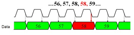
Figure 4 – Data Sampled Twice
Timing violation could also cause missing of samples. Sampling could also occur during the transition of data, which would give you completely erroneous data.
Synchronous Transfer
Synchronous transfer is when data is generated at a constant rate using a shared periodic clock. The data and control signals are generated relative to the clock edge.
Figure 5 – Synchronous Data Transfer
In source synchronous synchronization a common clock synchronizes communication. The transmitting device sends the clock signal to the receiving device. Devices with onboard (internal) clocks divide down the onboard clock to get the desired frequency. This, however, gives a course resolution. For finer resolution an external clock can be used where the DUT (Device Under Test), or other external device would provide the clock.
Figure 6 – Source Synchronous Data Transfer
In system synchronous synchronization, either the receiver provides the clock or a common clock source provides the clock signal to both the transmitting device and the receiving device.
Figure 7 – System Synchronous Data Transfer
The Clock to Out Time (tCO) is the time between the rising edge of the clock and the transition of data. The rising and falling edges of the clock are automatically adjusted according to when the Data/Valid signals are stable.
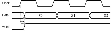
Figure 8 – Clock To Out Time (TCO)
SDR (Single Data Transfer) transfers data on only one clock transition (0-1 or 1-0); in contrast to DDR (Double Data Rate), two samples are taken every sample clock. DDR achieves higher bandwidth as by transferring data on both the rising and falling edge of the clock signal is used to allow higher speeds of transfer with slower hardware designs.
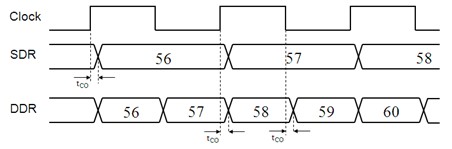
Figure 9 – SDR and DDR
Like DDR before it, DDR2 cells transfer data both on the rising and falling edge of the clock (a technique called double pumping). The key difference between DDR and DDR2 is that in DDR2 the bus is clocked at twice the speed of the memory cells, so four words of data can be transferred per memory cell cycle. Thus, without speeding up the memory cells themselves, DDR2 can effectively operate at twice the bus speed of DDR.
Asynchronous transfer
Asynchronous transfer is when data is sent using handshaking signals: There is no shared clock. Control signals synchronize communication between the two devices. Many different modes exist for asynchronous transfers.
Figure 10 – Asynchronous Transfer
The figure below displays an example of asynchronous data transfer. The transmitter outputs data within tDV after asserting the write signal. The receiver samples or latches data on the rising edge of the write signal.
Figure 11 – Asynchronous Data Transfer Example
Data Delay
Data Delay allows you to phase shift the acquisition channels, generation channels, and the exported clock. Configuring data and clock positions allows you to use your NI digital i/o instrument for many common applications including measuring setup and hold times, measuring propagation delays, and maximizing the timing margins among high-speed data transfers. Data Delay is available only on Synchronization and Memory Core (SMC) based digital products which include the NI 6541/42, 6551/52, and 6561/62 in either PCI or PXI.
The delay value can be as small as 1/256th of the clock frequency, and requires a minimum clock speed of 25 MHz (for frequencies below 25 MHz, oversample the data at a rate where clock delay is available). You can set each individual channel to apply the delay, or ignore it. You can choose one data delay value for generation and one for acquisition only per board. For example, you can delay your acquisition channels by 1/64 of your clock period, and delay your generation channels by only 1/256 of your clock period.
In addition to data delay, the NI SMC-based digital products above also allow you to set an additional clock delay called tCO to help offset reading data during a transition. This value is 2.5 ns and is enabled by default. You can turn this off or on per-channel while using the data delay setting.
The figure below shows data delay being used with generation. The data delay tDD(Tx), is added to the Clock to Out Time (tCO) to delay the data by the specified amount.
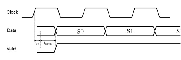
Figure 12 – Data Delay (Generation)
Data delay can be used with acquisition as well. In this case, the sample taken is delayed by tDD(Rx).
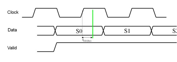
Figure 13 – Data Delay (Acquisition)
Jitter and Noise
Jitter is essentially noise in the time domain of a digital signal. The edges of a clock signal, for example, are not all exactly a constant time apart from each other. Each clock period varies by a small amount caused by small imperfections. This period-to-period error or variation is called jitter.
Skew is the time difference between two events that occur simultaneously. Inter-channel skew is an example of the time differences introduced by different characteristics of multiple channels.
Skew can occur between channels on one module, or between channels on separate modules (inter-module skew).
The setup time (Tsu) is the amount of time that the data signal must be stable before the assertion edge of the clock. The holt time (TH) is the amount of time that the data signal must be stable after the assertion edge of the clock.
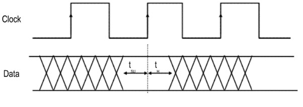
Figure 14 – Setup Time and Hold Time
The Real Picture
Apart from the Clock to Out Time and the Transmit Data Delay (TDD(Tx)) and the Receive Data Delay (TDD(Rx)), there are also other parameters that affect the actual delay in synchronization. The above mentioned setup time and hold time are such parameters.
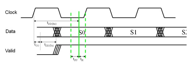
Figure 15 – The Real Picture