Using SPI with LabVIEW and the USB-8451
Overview
The SPI bus is a four-wire, full-duplex serial interface. SPI specifies four signals, clock (SCLK), master output, slave input (MOSI); master input, slave output (MISO); and chip/slave select (SS). SCLK is generated by the master and input to all slaves. MOSI carries data from master to slave. MISO carries data from slave back to master. A slave device is selected when the master asserts its SS signal.
Communication across SPI uses a system known as data exchange. Whenever a bit is written to an SPI device across the MOSI lines, the SPI device concurrently returns a bit on the MISO line. Because data is transferred in both directions, it is up to the receiving device to know whether the received byte is meaningful or not. For example, to receive data from an EEPROM, the master must configure the EEPROM to send n bytes of data and then must send n bytes to be exchanged for valid data. These bytes can usually be any value, and writing them serves only to clock the data out of the receiving device.
Contents
Terminology
| CLK | Clock, The clock is generated by the master device and controls when data is sent and read |
| MOSI | Master Output, Slave Input. The MOSI line carries data from the master to the slave |
| MISO | Master Input, Slave Output. The MISO carries data from the slave to the master |
| CS or SS | Chip Select or Slave Select. Connection from the master to a slave that signals the slave to listen for SPI clock and data signals |
| CPOL | Clock Polarity, The polarity indicates whether the clock makes positive or negative pulses |
| CPHA | Clock Phase, This controls the positioning of the data bits relative to the clock edges |
ERROR Handling
Unlike I2C, SPI has no acknowledgement mechanism or flow control. This prevents the SPI master from knowing whether a slave received a data byte correctly or even whether it is connected to the bus.
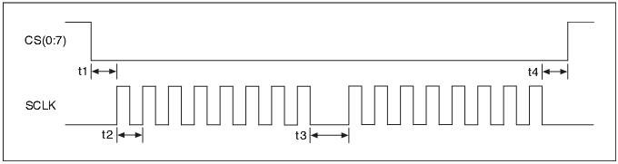
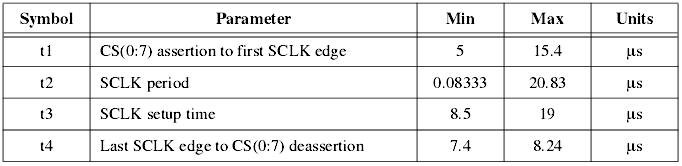
SPI Timing Characteristics
The Table below shows the timing characteristics of the SPI bus when using the SPI Basic API. A graph displaying the timing characteristics for SPI is shown in Figure 1. The table in Figure 1 shows the acceptable range for the parameters shown in the graph. If the timing characteristics of your device do not fit within these parameters, you can use the SPI Advanced API to adjust the bus characteristics to match those of your device.
Clock Polarity and Phase
Parameters called clock polarity (CPOL) and clock phase (CPHA) determine the clock idle state and the edge of the clock signal when the data on MISO or MOSI is driven or sampled. These parameters are sometimes expressed as four modes, as shown below.
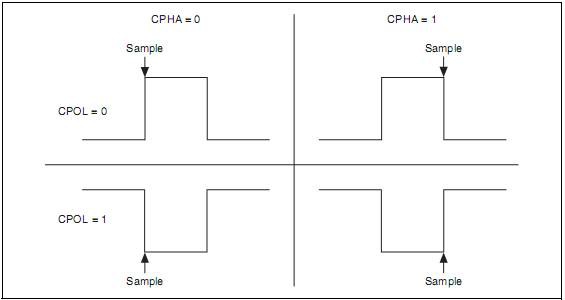
- When CPOL=0 the clock idles low (zero)
- CPHA=0: Data is read on the clock's rising edge (low to high clock transition). Data is also changed on a falling edge (high to low clock transition).
- CPHA=1: Data is read on the clock's falling edge (high to low clock transition). Data is also changed on a rising edge (low to high clock transition).
- When CPOL=1 the clock idles high (one)
- CPHA=0: Data is read on the clock's falling edge (high to low clock transition). Data is also changed on a rising edge (low to high clock transition).
- CPHA=1: Data is read on the clock's rising edge (low to high clock transition). Data is also changed on a falling edge (high to low clock transition).
Programming Model
The SPI Basic API provides the most fundamental SPI transaction types: read and write. You can access most off-the-shelf SPI devices using these transactions. The SPI Basic API allows you to easily and quickly develop applications to communicate with these devices. For those situations in which the SPI Basic API does not provide the functionality needed, use the SPI Advanced API to create custom SPI transactions.
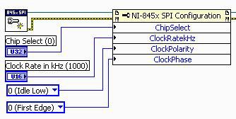
When using the SPI Basic API, the first step is to create a SPI configuration to describe the communication requirements between the 845x and the SPI device including the Chip Select device addressing. To make a SPI configuration, create a SPI configuration reference and set the appropriate properties as desired. This is demonstrated in the following section.
When you use the SPI Advanced API, the first step is to create a script that describes the communication between an SPI master and an SPI slave device including the Chip Select device addressing. Then you execute the script and extract the read data if needed. The script size is limited only by the amount of memory available on your PC. The number of read commands, SPI Script Write Read, SPI Script DIO Read Port, and SPI Script DIO Read Line within each script is limited to 64. Within the application, you repeat this programming model for each SPI device.
Basic LabVIEW API for Device Addressing
Use the NI-845x SPI Configuration Node to enter the chip select device address. Additionally you need to specify the clock rate, phase and polarity. You can select these properties by right clicking on the Configuration Node Property, selecting Select Property in the menu, and then selecting the desired property. The configuration output goes then to the high level Write/ Read VI.
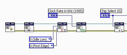
Advanced LabVIEW API for Device Addressing
Use the Script Clock Polarity/Phase + Clock Rate or + Chip Select Low after a Script Issue Start to configure the device for communication.
Write Operations
There are two kind of Write operations:
- Byte write
- Page write
Byte Write
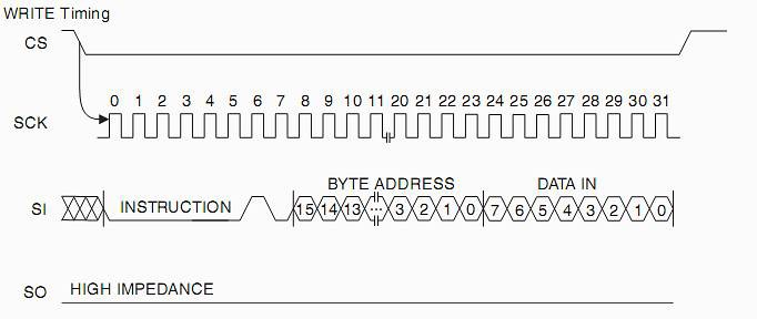
A write operation requires the following sequence. After the CS line is pulled low to select the device, the optional instruction-code is transmitted via the MOSI line followed by the byte address (A15-A0) and the data (D7–D0) to be programmed (see Figure 5). Programming will start after the CS pin is brought high again. The low-to-high transition of the CS pin must occur during the SCK low-time immediately after clocking in the D0 (LSB) data bit.
Page Write
Most EEPROMs are capable of a page write operations. After each byte of data is received, the address bits are internally incremented by one. The device is automatically returned to the write disable state at the completion of a write cycle.
Note: You need to look at the page size of your chip! Page Write operations are limited to writing bytes within a single physical page, regardless of the number of bytes actually being written. Physical page boundaries start at addresses that are integer multiples of the page buffer size (or ‘page size’) and end at addresses that are integer multiples of
[page size – 1].
If a Page Write command attempts to write across a physical page boundary, the result is that the data wraps around to the beginning of the current page (overwriting data previously stored there), instead of being written to the next page as might be expected. It is therefore necessary for the application software to prevent page write operations that would attempt to cross a page boundary.
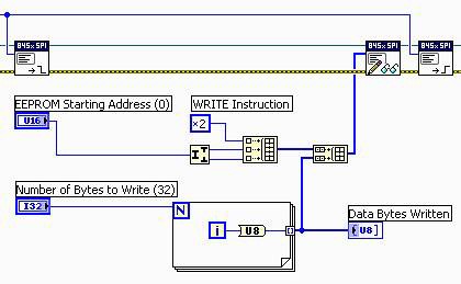
Basic LabVIEW API for Write Operations
The basic write operation takes the device descriptor, the configuration reference (including the device address) and uses a data byte array to write the instruction byte and the data bytes to the address specified in the first two bytes.
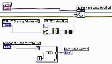
Note: To write to single byte addresses use a single U8 integer instead of the U16 for the address.
Advanced LabVIEW API for Write Operations
Use the Script write function to write the instruction byte and the data bytes to the address specified in the first two bytes, to have the same result as using the basic function.
Read Operations
Read operations are initiated in the same way as write operations. There are three basic types of read operations:
- current address read
- random read
- sequential read
Current Address Read
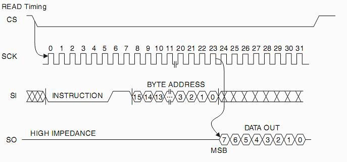
Reading via the Serial Output (MISO) pin requires the following sequence. After the CS line is pulled low to select a device, the optional read op-code is transmitted via the MOSI line followed by the byte address to be read (A15–A0, see Figure 8). Upon completion, any data on the SI line will be ignored. The data (D7–D0) at the specified address is then shifted out onto the MISO line. If only one byte is to be read, the CS line should be driven high after the data comes out.
Random Read
Random Read operations allow the USB-8451 to access any memory location in a random manner. To perform this type of read operation, the random address must be set within the data bytes.
After a Random Read command, the internal address counter will point to the address location following the one that was just read. If only one byte is to be read, the CS line should be driven high after the data comes out.
Sequential Read
A read sequence can be continued since the byte address is automatically incremented and data will continue to be shifted out.
When the highest address is reached, the address counter will roll over to the lowest address allowing the entire memory to be read in one continuous read cycle.
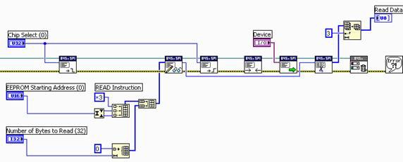
Basic API for Read Operations
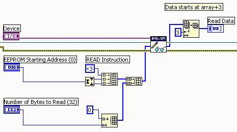
The basic write/read operation takes the device descriptor, the configuration reference (including the device address) and uses a data byte array to write the optional instruction byte and the data bytes to the address specified in the first two bytes. At the same time it reads the data bytes back on MISO. Keep in mind that the data comes with the offset of three because we had to send 3 more bytes for instruction and address.
Note: To read from a single byte address, use a single U8 integer instead of the U16 for the address.
Advanced API for Read Operations
Use the Script write/read function to write the instruction byte and the data bytes to the address specified in the first two bytes, to have the same result as using the basic function. Keep in mind that the data comes with the offset of three because we had to send 3 more bytes for instruction and address.
Note: To read from a single byte address, use a single U8 integer instead of the U16 for the address.