From Friday, April 19th (11:00 PM CDT) through Saturday, April 20th (2:00 PM CDT), 2024, ni.com will undergo system upgrades that may result in temporary service interruption.
We appreciate your patience as we improve our online experience.
From Friday, April 19th (11:00 PM CDT) through Saturday, April 20th (2:00 PM CDT), 2024, ni.com will undergo system upgrades that may result in temporary service interruption.
We appreciate your patience as we improve our online experience.
This tutorial is part 1 of a three part series that discusses switching low-level voltage,current, and resistances. Each tutorial in this series, will provide you with insights on low-level switching for various different applications and measurement types. This tutorial introduces and discusses the techniques and challenges when switching low-voltage signals.
The other tutorials in this series are:
An ideal switching system is one that can route signals from one location to another without hindering the integrity of that signal. To replicate such a system in the real world is unattainable. Any switch added in the path of a signal will degrade that signal to some extent. A good switching system will cause minimum degradation while a bad one can have significantly larger effects. The quality of a switching system is especially important when switching low-level signals because measuring low-level signals accurately is an intricate procedure where numerous factors such as circuit parasitics and imperfections in relays can account for huge percentage errors.
To expand on this concept, let us consider a relay used to route a 5 μV signal to a digital multimeter. If the thermal emf (voltage induced due to contact of 2 dissimilar metals) of that relay is 2 μV, then the voltage measured by the instrument will be between 3 and 7 μV due to the fact that induced error will be between -2 and +2 μV. Hence, it can be seen that in this particular case the addition of one relay in the signal path caused a 40 percent error in the measurement of that signal. In the same fashion that thermal emf affects low-voltage switching, factors such as leakage current and switch path resistance affect current and resistance measurements respectively. This white paper will address chief concerns associated with switching signals for the purpose of current, voltage, and resistance measurements. It will also provide pointers and precautionary measures that should be followed in order to reduce measurement errors and improve accuracy when measuring low-level signals through a switch.
Depending on the application, a low voltage signal can range anywhere from a few nanovolts to a few millivolts. To route such signals between different locations can be challenging, mainly because even a small error voltage in the switching system can substantially affect the integrity of a signal being routed through it. Voltage offsets in a switching system are mainly caused by the thermal emf of a particular switch, noise and interference from the environment, and switch path resistance. A detailed explanation of each of these phenomena along with ways to reduce their effects is discussed in this section.
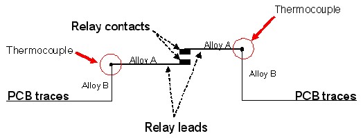
Electromechanical relays use magnetic fields generated by a coil to switch between OPEN and CLOSED states. When the coil is energized the relay contacts meet thus completing the circuit. In a switch module, relays are usually laid out on a PCB. Signals enter the switch module through a front connector. From here they are routed to the relay via a carved trace on the PCB. After passing through the relay, the signals make their way to the switch module output via another PCB trace. The input terminal, PCB traces, and output all form a part of the signal path. In the case of all switch modules, this signal path consists of several junctions where two dissimilar metals meet and thus form thermocouples. An example of such a junction would be where the leads of a relay come in contact with the PCB trace which is more often than not made of a different metal than the leads themselves (Refer to Figure 2).
Figure 1. Thermocouple Created at Junction of Relay Lead and PCB Trace
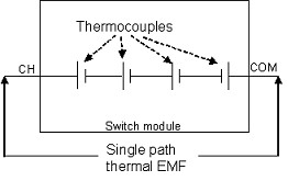
The voltage created by these thermocouples depends on several factors such as ambient temperature, the number of relays and air flow inside the module. The total voltage generated by all thermocouples in a signal path is referred to as thermal emf.
Figure 2. Total Thermal EMF of a Switch Module
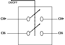
The effects of thermal emf can be minimized by using a differential measurement setup in which the high and low terminals of the source signal both pass through a channel on the switch module. Since both channels on the switch module have close to equivalent thermal emfs, their voltage offsets cancel each other out and thus reduce the net thermal emf induced in the system. When making differential measurements it is often advantageous to use switch modules that have double-pole single-throw (DPST) relays. Such relays consist of two SPST (single pole single throw) relays that open and close at the same time (refer to Figure 3). These SPST relays are contained in a single housing package which ties them together thermally. Thus any external factor (for example, change in ambient temperature) that affects the thermal condition of one relay will do the same to the other. In addition to having the stated benefits, SPST relays used in a DPST relay come from the same manufacturing batch which helps reduce differences in their material properties. All of these reasons combined make it more plausible for SPST switches in DPST form to have minimal differences in their thermal emf.
Figure 3. Double-Pole Single-Throw (DPST) Relays
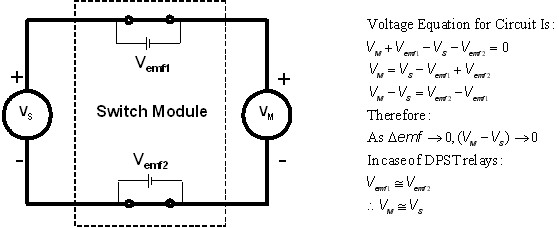
It is impossible for two relays to have the exact same thermal emf. However, DPST switches can help minimize this difference when used in differential measurements. In the circuit below, let us assume that the thermal emf of the first relay is Vemf1 and the thermal emf of the second relay is Vemf2 , the source voltage is VS, and the voltage measured is VM. Then:
Figure 4. Differential Measurement Using Two Relays
It is important to note that absolute cancellation of thermal emf never takes place. Even in the case of DPST relays, there is a slight difference in thermal emf between the two relays. However differential measurements with DPST relays can help significantly reduce voltage offsets in measurements caused by thermal emf.
To reduce the consequences of thermal emf when using nonlatching relays, it is often wise to take measurements within a few seconds after the relay is closed because these relays need a constant current to be supplied to them in order to maintain a given state or position. This constant current supply causes power to be dissipated by the relay coil which in turn causes the temperature to rise creating a thermal gradient for several minutes after the relay is closed. The higher the gradient, the higher the voltage associated with thermal emf. This phenomenon is much less prevalent in the case of latching relays which stay in a particular position without the need for continuous current supply.
Lastly, it is always advisable to use wiring made of the same metal as the PCB connectors and traces. Using a uniform metal across the signal path reduces offsets caused due the creation of thermocouples and thus improves accuracy. In general, most PCB traces are made of copper in which case using copper cabling is a good option. However, in the case that a PCB is plated with a metal other than copper, the process of choosing appropriate wiring may not be pragmatic.

Contact resistance (a subset of path resistance) of a relay which is the DC resistance through one set of closed contacts in a relay, increases over time. Due to wear and tear of the relay, a contamination layer forms on the surface of its contacts increasing its contact resistance and thus the voltage drop across that relay. In general, a newer switch will add less error to a signal path than an older one. Refer to switch product documentation to determine specifications such as relay lifetime. Using features such as relay count tracking, available on most NI switch modules, can also help determine if contact resistance of a relay is at an acceptable level for the application. It is important to note that the concept of contact resistance of a relay increasing over its lifetime applies only to electromechanical relays which have moving parts unlike FETs and SSRs. Lastly, because all cables have some resistance associated with them, using shorter cables can help reduce effective path resistance thus minimizing erroneous potential drops in the signal path.
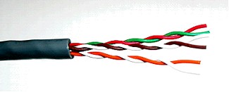
Sources of noise can include objects that may carry a current in close proximity to the test system. Examples of such objects include bur are not limited to heavy machinery and fluorescent lighting. Because of the sensitivity of the measurement, circuits switching low-voltage signals should be decoupled from noise sources to the maximum extent possible to minimize the effects of charge transfer from these sources. Furthermore, in order to protect signals from the influence of noise in the signal path, it is also advisable to use shielded and twisted-pair cables. Twisted-pair cables have the ability to cancel out electromagnetic interference and reduce cross talk between channels.
Figure 5. Twisted-Pair Cables with Shield
To reduce measurement errors when routing low-voltage signals, always use shielded and twisted pair cables that are made of the same metal or material as the connector on the switch module. Such cables improve isolation of the signal path and thus reduce errors induced by cross talk from neighboring sources. Lastly, try to choose a switch module that has low thermal emf (less than 5 μV) and path resistance (less than 1 Ω).
View Part II and Part III of this tutorial series to learn more about low-level switching:
Customers interested in this topic were also interested in the following NI products: