Digital Timing: Clock Signals, Jitter, Hystereisis, and Eye Diagrams
Overview
Learn about digital timing of clock signals and common terminology such as jitter, drift, rise and fall time, settling time, hysteresis, and eye diagrams.
Contents
Clock Signals
When sending digital signals, a 0 or 1 is being sent. However, for different devices to communicate, timing information needs to be associated with the bits sent. Digital waveforms are referenced to clock signals. You can think of a clock signal as a conductor that provides timing signals to all parts of a digital system so that each process may be triggered at a precise moment.
A clock signal is a square wave with a fixed period. The period is measured from the edge of one clock to the next similar edge of the clock; most often is it measured from one rising edge to the next. The frequency of the clock can be calculated by the inverse of the clock period.
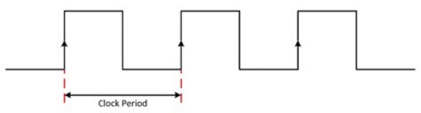
Figure 1: Digital waveforms are referenced to clock signals, which have a fixed period to synchronize digital transmitters and receivers during data transfer.
The duty cycle of a clock signal is the percentage of the waveform period that the waveform is at a logic high level. Figure 2 shows the difference between two waveforms with different duty cycles. You can see that the 30 percent duty cycle waveform is at a logic high level for less time than the 50 percent duty cycle.
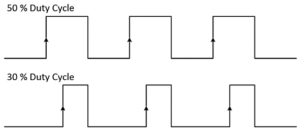
Figure 2: The duty cycle of a signal is the percentage of time the waveform is at a logic high level.
Clock signals are used to synchronize digital transmitters and receivers during data transfer. For example, the transmitter can use each rising edge of the clock signal to send each bit of data and the receiver can use the same clock to read the data. In this scenario, the assertion edge of the device is the rising edge (low to high). For other devices, it is the falling edge (high to low). The assertion edge of the clock is also called the active clock edge. Digital transmitters drive new data samples on each active clock edge while receivers sample data on each active clock edge. Newer devices are beginning to use both the rising and falling edge of the clock; these are called double date rate (DDR) devices. In actuality, the data is transmitted after a small delay from the assertion edge of the clock; this delay is called the clock-to-out time.
When a receiver samples the data on the digital lines, there are two timing parameters to be aware of in order to receive data reliably. Setup time (ts) is the amount of time the data must be at a valid logic level uninterrupted while the receiver sets itself up to receive the input. The hold time (tH) specifies the amount of time the data needs to hold the state before the it can change after it has been sampled by the receiver. Together, the setup time and hold time set up a stable window around the assertion edge of the receiver’s clock for the receiver to reliably sample the data. Figure 3 shows setup and hold times with reference to a rising-edge clock signal. Often, digital signals switch the voltage midway between the supply rails; for this reason, the time reference markers are positioned at the midpoint of the signal edges.
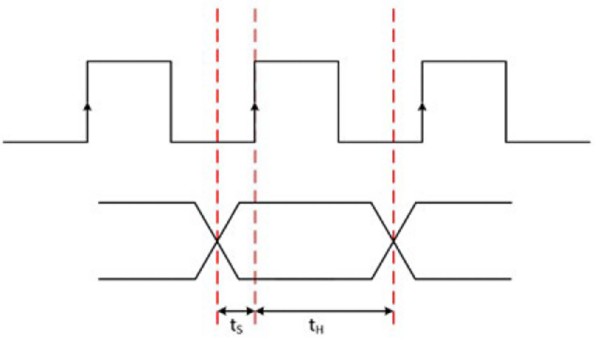
Figure 3: The duty cycle of a signal is the percentage of time the waveform is at a logic high level.
Common Terminology
In digital systems, timing is one of the most important factors. The reliability and accuracy of digital communications are based on the quality of its timing. However, in the real world, nothing is ever ideal. Below are some common terms and ways to better understand the timing of your particular digital signal.
Jitter
Jitter is the deviation from the ideal timing of an event to the actual timing of an event. To understand what this means, imagine you are sending a digital sine wave and plotting it on graph paper. Each square corresponds to a clock pulse; because the vertical lines are equidistant apart, you end up with a perfectly periodic clock signal. At each clock pulse, you receive three bits and plot that point on your graph paper. Because of the periodic nature, it ends up as a nice sine wave.
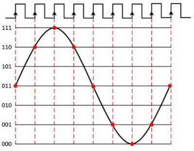
Figure 4: A sample clock that is periodic allows a digital system to communicate correctly and accurately.
Now, imagine that those lines aren’t equidistant apart. This would make your clock signal less periodic. When you plot your data, it isn’t at the same intervals and, thus, doesn’t look correct.
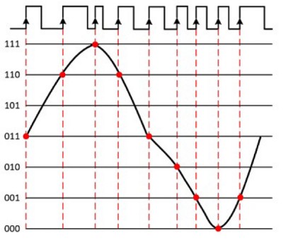
Figure 5: If a clock signal has jitter, it results in distortion of the digital waveform.
In Figure 5, you can see that the distance between the transitions in the clock signal is uneven; this is jitter in the clock. Although the above figure has an exaggerated amount of jitter, it does show how a jittery clock can cause samples to be triggered at uneven intervals. This unevenness introduces distortion into the waveform you are trying to record and reproduce.
Now look at jitter in terms of a digital signal with only 1s and 0s. Remember, jitter is the deviation from the ideal timing of an event to the actual timing of an event. Taking a look at a single pulse, jitter is the deviation in edge timing from the actual signal to the ideal positions in time.
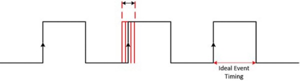
Figure 6: Jitter of a single pulse is the deviation in edge timing.
Jitter is typically measured from the zero-crossing of a reference signal. It typically comes from cross-talk, simultaneous switching outputs, and other regularly occurring interference signals. Jitter varies over time, so measurements and quantification of jitter can range from a visual estimate on an oscilloscope in the range of jitter in seconds to a measurement based on statistics such as the standard deviation over time.
Drift
Another common timing issue is drift. Clock drift occurs when the transmitter’s clock period is slightly different from that of the receiver. At first, it may not make much of a difference. However, over time, the difference between the two clock signals may become noticeable and cause loss of synchronization and other errors.
Rise Time, Fall Time, and Aberrations
Even with drift, in theory, when a digital signal goes from a 0 to a 1, it would happen instantaneously. However, in reality, it takes time for a signal to change between high and low levels. Rise time (trise) is the time it takes a signal to rise from 20 percent to 80 percent of the voltage between the low level and high level. Fall time (tfall) is the time it takes a signal to fall from 80 percent to 20 percent of the voltage between the low level and high level.
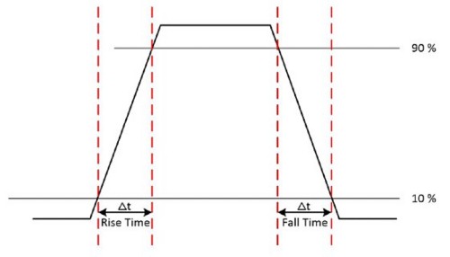
Figure 7: Rise time and fall time indicate the length of time a signal takes to change voltage between the low level and high level.
In addition, in the real world, a signal rarely hits a voltage level and stays there in a clean fashion. When a signal actually exceeds the voltage level following an edge, the peak distortion is called overshoot. If the signal exceeds the voltage level preceding an edge, the peak distortion is called preshoot. In between edges, if the signal drifts short of the voltage level it is called undershoot.
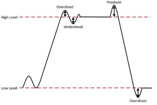
Figure 8: Overshoot, preshoot, and undershoot are collectively called aberrations.
Together, overshoot, preshoot, and undershoot are called aberrations. Aberrations can result from board layout problems, improper termination, or quality problems in the semiconductor devices themselves.
Settling Time
After a digital signal has reached a voltage level, it bounces a little and then settles to a more constant voltage. The settling time (ts) is the time required for an amplifier, relay, or other circuit to reach a stable mode of operation. In the context of digital signal acquisition, the settling time for full-scale step is the amount of time required for a signal to reach a certain accuracy and stay within that range.
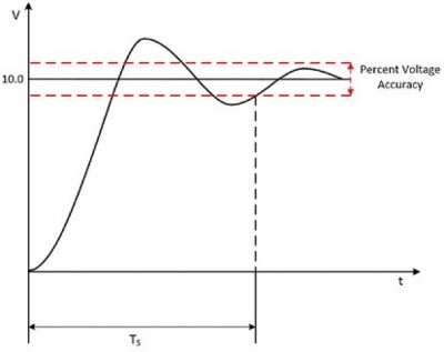
Figure 9: Settling time is the amount of time for a signal to reach a certain accuracy and stay within that range.
Hysteresis
Hysteresis refers to the difference in voltage levels between the detection of a transition from logic low to logic high, and the transition from logic high to logic low. It can be calculated by subtracting the input high voltage from the input low voltage.
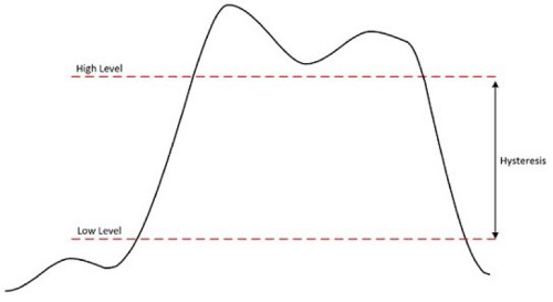
Figure 10: Hysteresis is the difference in voltage levels between the detection of a transition from one logic value to another.
Hysteresis is a useful property for digital devices, because it naturally provides some amount of immunity to high-frequency noise in your digital system. This noise, often caused by reflections from the high-edge rates of logic level transitions, could cause the digital device to make false transition detections if only a single voltage threshold determined a change in logic state. You can see this in Figure 11. The first sample is acquired as a logic low level. The second sample is also a logic low level because the signal has not yet crossed the high-level threshold. The third and fourth samples are logic high levels, and the fifth is a logic low level.
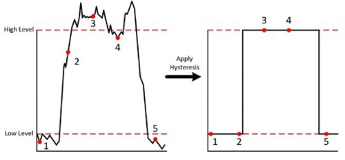
Figure 11: Hysteresis provides an amount of immunity to high-frequency noise in your digital system.
For devices with fixed voltage thresholds, the noise immunity margin (NIM) and hysteresis of your system are determined by your choice of system components. Both system NIM and hysteresis give your system levels of noise immunity, but for a specific logic family, there is always a trade-off between these two—the larger the hysteresis, the smaller the NIM, and vice versa. To determine how to set your voltage thresholds, you should carefully examine the signal quality in your system to determine whether you need more noise immunity from your high and low logic levels (greater NIM) or need more noise immunity on your logic level transitions (greater hysteresis).
Skew
Skew is when the clock signal arrives at different components at different times. Unlike drift, the clock signals have the same period; they just arrive at different times. This can be caused by a variety of factors including wire length, temperature variation, or differences in input capacitance. Channel-to-channel skew generally refers to the skew across all data channels on a device. When each sample is acquired, the point in time at which each data channel is sampled with respect to every other data channel is not identical, but the difference is within some small window of time called the channel-to-channel skew.
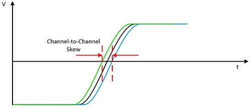
Figure 12: Channel-to-channel skew generally refers to the skew across all data channels on a device.
Eye Diagram
An eye diagram is a timing analysis tool that provides you with a good visual of timing and level errors. In real life, errors, like jitter, are difficult to quantify because they change so often and are so small. Therefore, an eye diagram is an excellent tool for finding the maximum jitter as well as measuring aberrations, rise times, fall times, and other errors. As these errors increase, the white space in the center of the eye diagram decreases.
An eye diagram is created by overlaying sweeps of different segments of a digital signal. It should contain every possible bit sequence from simple high to low transitions to isolated transitions after long runs of consistency. When overlapped, it looks like an eye. Eye diagrams are a visual way to understand the signal integrity of a design. Keep in mind that an eye diagram shows parametric information about a signal, but does not detect logic or protocol problems such as when it is supposed to transmit a high but sends a low.
Figure 13 shows common terminology of an eye diagram.
A. High level, also called the one level, is the main value of a logic high. The calculated value of a high level comes from the mean value of all the data samples captured in the middle 20 percent of the eye period.
B. Low level, also called the zero level, is the main value of a logic low. This level is calculated in the same region as the high level.
C. Amplitude of the eye diagram is the difference between the high and low levels.
D. Bit period, also referred to as the unit interval (UI), is a measure of the horizontal opening of an eye diagram at the crossing points of the eye. It is the inverse of the data rate. When creating eye diagrams, using the bit period on the horizontal axis instead of time, gives you the ability to compare diagrams with different data rates easily.
E. Eye height is the vertical opening of an eye diagram. Ideally, this would equal the amplitude, but this rarely occurs in the real world because of noise. As such, the eye height is smaller the more noise in the system. The eye height indicates the signal-tonoise ratio of the signal.
F. Eye width is the horizontal opening. It is calculated as the difference between the statistical mean of the crossing points of the eye.
G. Eye crossing percentage shows duty cycle distortion or pulse symmetry problems. An ideal signal is 50 percent; as the percentage deviates, the eye closes and indicates degradation of the signal.
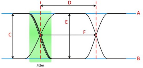
Figure 13: The image shows the high level (A), low level (B), amplitude (C), bit period (D), eye height (E), eye width (F), and eye crossing percentage (G) on an eye diagram.
Figure 14 shows additional measurements on an actual eye diagram.
A. Rise time in the diagram is the mean of the individual rise times. The slope indicates sensitivity to timing error; the smaller the better.
B. Fall time in the diagram is the mean of the individual fall times. The slope indicates sensitivity to timing error; the smaller the better.
C. The width of the logic high value is the amount of distortion in the signal (set by the signal-to-noise ratio).
D. The signal-to-noise ratio at the sampling point is from the eye width to the bottom or the logic high-voltage range.
E. Jitter of the signal.
F. The most open part of the eye is when there is the best signal-to-noise ratio and is thus the best time to sample.
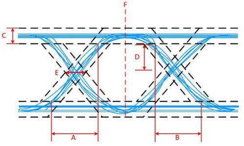
Figure 14: The image shows the rise time (A), fall time (B), distortion (C), signal-to-noise ratio (D), jitter (E), and best time to sample (F) on an eye diagram.
Summary
- Digital waveforms are referenced to clock signals, which have a fixed period to synchronize digital transmitters and receivers during data transfer.
- The duty cycle of a clock signal is the percentage of the waveform period that the waveform is at logic high level.
- The assertion edge of the clock is called the active clock edge.
- The setup time and hold time set up a stable window around the assertion edge of the receiver’s clock for the receiver to reliably sample the data.
- Jitter is the deviation from the ideal timing of an event to the actual timing of an event; jitter in timing can cause distortion in the signal.
- Clock drift occurs when the transmitter’s clock period is slightly different from that of the receiver and can cause loss of synchronization and other errors.
- Rise time and fall time indicate the length of time a signal takes to change voltage between the low level and the high level.
- Overshoot, preshoot, and undershoot are called aberrations and are an indication of errors in the system.
- Settling time is the amount of time for a signal to reach a certain accuracy and stay within that range.
- Hysteresis provides an amount of immunity to high-frequency noise in your digital system.
- Skew is when the clock signal arrives at different components at different times.
- An eye diagram is a timing analysis tool that provides you with a good visual of timing and level errors.
Next Steps
- Learn about NI digital instruments for automated characterization, validation, and production test
- Explore additional NI digital I/O products for data acquisition and control
- Learn about VirtualBench, an all-in-one instrument for interactive benchtop design and validation
- Download all instrument fundamentals content