Data Transfer Using Panel Controls and Indicators
- Updated2023-02-17
- 2 minute(s) read
Data Transfer Using Panel Controls and Indicators
Note Support for
programmatic panel communication varies for each FPGA target. Refer to the hardware
documentation for the FPGA target for more information.
Use this method for small, frequent data transfers between the FPGA and the host because each call to the Read Write FPGA Control node initiates data transfer with minimal delay and low overhead. This method transfers only the most current data stored on the control or indicator of the FPGA VI.
Note To transfer data between the FPGA and
the host without data loss, use
FIFOs instead.
What to Use
What to Do
Create the following diagram in a VI targeted to your host processor.
Customize the gray section for your unique programming goals.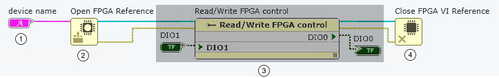

|
Use the device name for your FPGA found in SystemDesigner to specify an FPGA target. To ensure your code runs on the FPGA, the device name input must match the FPGA device name. |

|
Select the Open FPGA Reference node and select a mode of assigning an FPGA bitfile or application on the Item tab. To obtain a bitfile, you must compile FPGA code into a bitfile. |

|
Select the controls or indicators in the FPGA VI that you want to read or write using the Read Write FPGA Control node. Resize the node to access more elements. To switch between read and write operations for an element, right-click the element and select Change to Read/Write. |

|
Use the Close FPGA VI Reference node to close every reference the Open FPGA Reference node creates. |