FPGA Fundamentals: Basics of Field-Programmable Gate Arrays
Overview
Contents
Unlike processors, FPGAs are truly parallel in nature, so different processing operations do not have to compete for the same resources. Each independent processing task is assigned to a dedicated section of the chip and can function autonomously without any influence from other logic blocks. As a result, the performance of one part of the application is not affected when you add more processing.
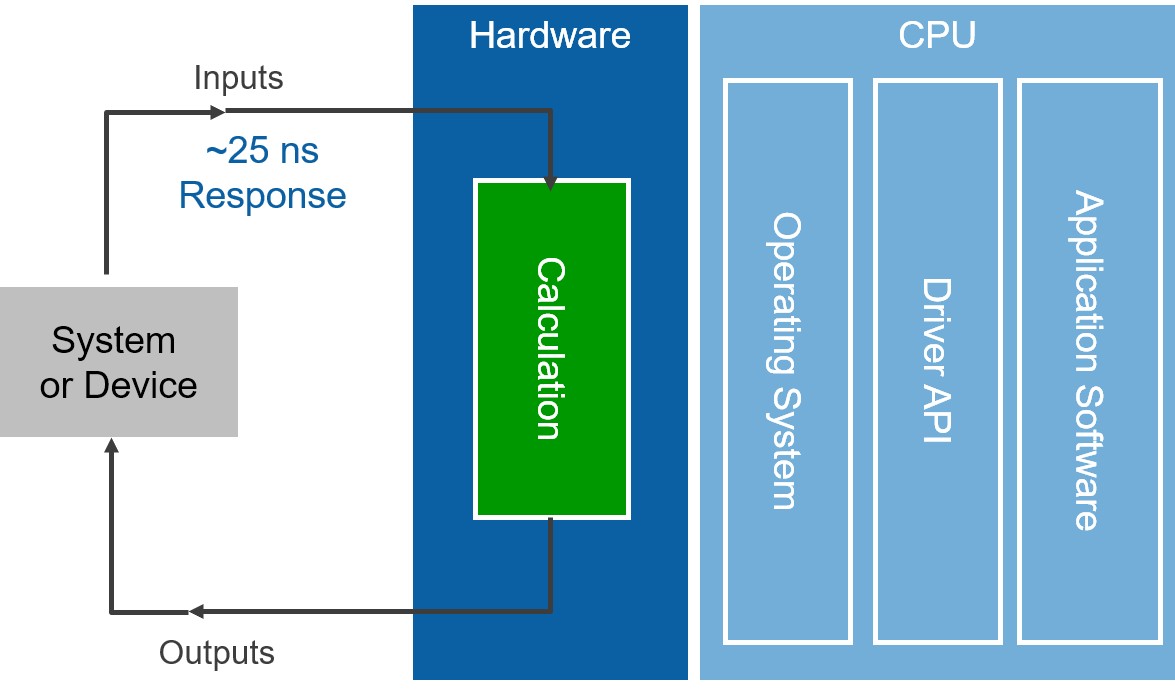
Figure 1: One of the benefits of FPGAs over processor-based systems is that the application logic is implemented in hardware circuits rather than executing on top of an OS, drivers, and application software.
Defining the Parts of an FPGA
Every FPGA chip is made up of a finite number of predefined resources with programmable interconnects to implement a reconfigurable digital circuit and I/O blocks to allow the circuit to access the outside world.
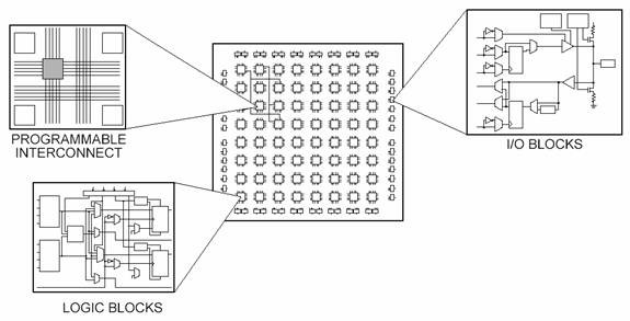
Figure 2: The Different Parts of an FPGA
FPGA resource specifications often include the number of configurable logic blocks, number of fixed function logic blocks such as multipliers, and size of memory resources like embedded block RAM. Of the many FPGA specifications, these are typically the most important when selecting and comparing FPGAs for a particular application.
The configurable logic blocks (CLBs) are the basic logic unit of an FPGA. Sometimes referred to as slices or logic cells, CLBs are made up of two basic components: flip-flops and lookup tables (LUTs). Various FPGA families differ in the way flip-flops and LUTs are packaged together, so it is important to understand flip-flops and LUTs.
Flip-Flops
Flip-flops are binary shift registers used to synchronize logic and save logical states between clock cycles within an FPGA circuit. On every clock edge, a flip-flop latches the 1 or 0 (TRUE or FALSE) value on its input and holds that value constant until the next clock edge.
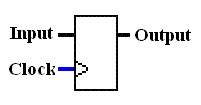
Figure 3: Flip-Flop Symbol
Flip-flops are binary shift registers used to synchronize logic and save logical states between clock cycles within an FPGA circuit. On every clock edge, a flip-flop latches the 1 or 0 (TRUE or FALSE) value on its input and holds that value constant until the next clock edge.
Lookup Tables (LUTs)
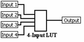
Figure 4: Four-Input LUT
Much of the logic in a CLB is implemented using very small amounts of RAM in the form of LUTs. It is easy to assume that the number of system gates in an FPGA refers to the number of NAND gates and NOR gates in a particular chip. But, in reality, all combinatorial logic (ANDs, ORs, NANDs, XORs, and so on) is implemented as truth tables within LUT memory. A truth table is a predefined list of outputs for every combination of inputs.
Here is the quick refresher from digital logic class.
The Boolean AND operation, for example, is shown in Figure 5:
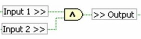
Figure 5: NI LabVIEW Boolean AND Operation
The corresponding truth table for the two inputs of an AND operation is shown in Table 1.

Input 1 | Input 2 | Output |
0 | 0 | 0 |
0 | 1 | 0 |
1 | 0 | 0 |
1 | 1 | 1 |
Table 1: Truth Table for Boolean AND Operation
Multipliers and DSP Slices
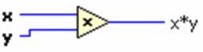
Figure 6: NI LabVIEW Multiply Function
The seemingly simple task of multiplying two numbers together can get extremely resource intensive and complex to implement in digital circuitry. To provide some frame of reference, Figure 6 shows the schematic drawing of one way to implement a 4-bit by 4-bit multiplier using combinatorial logic.
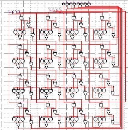
Figure 7: Schematic Drawing of a 4-Bit by 4-Bit Multiplier
Now imagine multiplying two 32-bit numbers together, and you end up with more than 2000 operations for a single multiply. Because of this, FPGAs have prebuilt multiplier circuitry to save on LUT and flip-flop usage in math and signal processing applications.
Many signal processing algorithms involve keeping the running total of numbers being multiplied, and, as a result, higher-performance FPGAs like Xilinx Virtex-5 FPGAs have prebuilt multiplier-accumulate circuitry. These prebuilt processing blocks, also known as DSP48 slices, integrate a 25-bit by 18-bit multiplier with adder circuitry.
Block RAM
Memory resources are another key specification to consider when selecting FPGAs. User-defined RAM, embedded throughout the FPGA chip, is useful for storing data sets or passing values between parallel tasks. Depending on the FPGA family, you can configure the onboard RAM in blocks of 16 or 36 kb. You still have the option to implement data sets as arrays using flip-flops; however, large arrays quickly become expensive for FPGA logic resources. A 100-element array of 32-bit numbers can consume more than 30 percent of the flip-flops in a Virtex-II 1000 FPGA or take up less than 1 percent of the embedded block RAM. Digital signal processing algorithms often need to keep track of an entire block of data, or the coefficients of a complex equation, and without onboard memory, many processing functions do not fit within the configurable logic of an FPGA chip.
The inherent parallel execution of FPGAs allows for independent pieces of hardware logic to be driven by different clocks. Passing data between logic running at different rates can be tricky, and onboard memory is often used to smooth out the transfer using first-in-first-out (FIFO) memory buffers.
Designing FPGAs Into a System
While there are many advantages to FPGAs, such as speed, reliability, and flexibility, there are also trade-offs associated with FPGAs. FPGAs do not have the driver ecosystem and code/IP base that microprocessor architectures and OSs do. In addition, microprocessors coupled with OSs provide the foundation for file structures and communication to peripherals used for many, often essential, tasks such as logging data to disk.
As a result, over the last decade a hybrid architecture, sometimes called a heterogeneous architecture, has emerged in which a microprocessor is paired with an FPGA that is then connected to I/O. Modern FPGAs often combine logic gates with processors into a single chip called a System on Chip (SoC) for increased computing performance. This approach takes advantage of the benefits that both these targets offer.
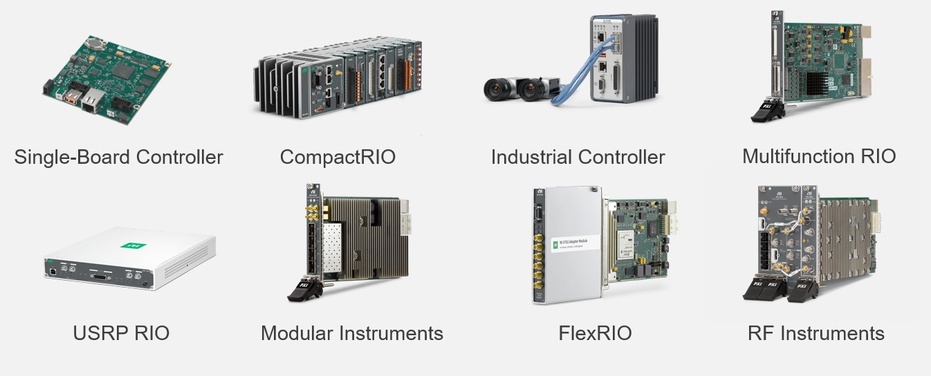
Figure 8: NI offers an entire family of FPGA-enabled devices both packaged and board-level that you can program with LabVIEW based on this ideal hybrid architecture coupling both a microprocessor and an FPGA.
National Instruments has implemented this powerful microprocessor plus FPGA architecture in its FPGA-enables devices. These devices span many different form factors, from rugged to high-performance systems, all based on this same architecture.
FPGA Design Tools
Now that you know the building blocks of an FPGA chip, you may ask, "How do you configure all of these millions of components to build up the logic that you need to execute?"
The answer is that you define digital computing tasks in software using development tools and then compile them down to a configuration file or bitstream that contains information on how the components should be wired together. The challenge in the past with FPGA technology was that the low-level FPGA design tools could be used only by engineers with a deep understanding of digital hardware design. However, the rise of high-level synthesis (HLS) design tools, such as LabVIEW, changes the rules of FPGA programming and delivers new technologies that convert graphical block diagrams into digital hardware circuitry.
Traditional FPGA Design Tools
Through the first 20 years of FPGA development, hardware description languages (HDLs) such as VHDL and Verilog evolved into the primary languages for designing the algorithms running on the FPGA chip. These low-level languages integrate some of the benefits offered by other textual languages with the realization that on an FPGA, you are architecting a circuit. The resulting hybrid syntax requires signals to be mapped or connected from external I/O ports to internal signals, which ultimately are wired to the functions that house the algorithms. These functions execute sequentially and can reference other functions within the FPGA. However, the true parallel nature of the task execution on an FPGA is hard to visualize in a sequential line-by-line flow. HDLs reflect some of the attributes of other textual languages, but they differ substantially because they are based on a dataflow model where I/O is connected to a series of function blocks through signals.
To then verify the logic created by an FPGA programmer, it is common practice to write test benches in HDL to wrap around and exercise the FPGA design by asserting inputs and verifying outputs. The test bench and FPGA code are run in a simulation environment that models the hardware timing behavior of the FPGA chip and displays all of the input and output signals to the designer for test validation. The process of creating the HDL test bench and executing the simulation often requires more time than creating the original FPGA HDL design itself.
Once you have created an FPGA design using HDL and verified it, you need to feed it into a compilation tool that takes the text-based logic and, through several complex steps, synthesizes your HDL down into a configuration file or bitstream that contains information on how the components should be wired together. As part of this multistep manual process, you often are required to specify a mapping of signal names to the pins on the FPGA chip that you are using.
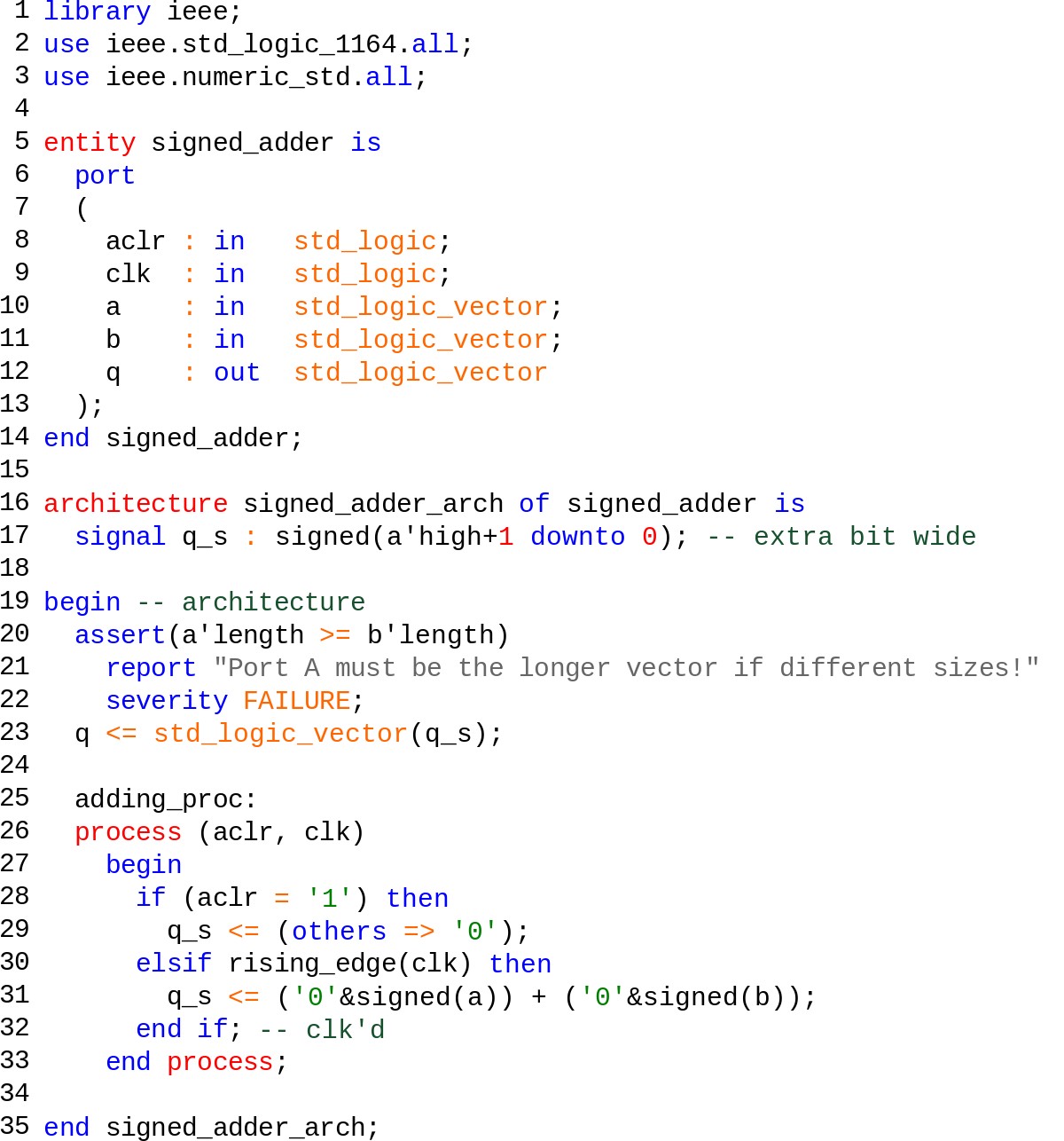
Figure 9: Simple Counter FPGA Design in VHDL
Ultimately, the challenge in this design flow is that the expertise required to program in traditional HDLs is not widespread, and as a result, FPGA technology has not been accessible to the vast majority of engineers and scientists.
High-Level Synthesis Design Tools
The emergence of graphical HLS design tools, such as LabVIEW, has removed some of the major obstacles of the traditional HDL design process. The LabVIEW programming environment is distinctly suited for FPGA programming because it clearly represents parallelism and data flow, so users who are both experienced and inexperienced in traditional FPGA design processes can leverage FPGA technology. In addition, so that previous intellectual property (IP) is not lost, you can use LabVIEW to integrate existing VHDL into your LabVIEW FPGA designs. Because LabVIEW FPGA is highly integrated with hardware, there is no need to rewrite code in VHDL to meet timing or resource constraints, as may be the case in many HLS code generators.
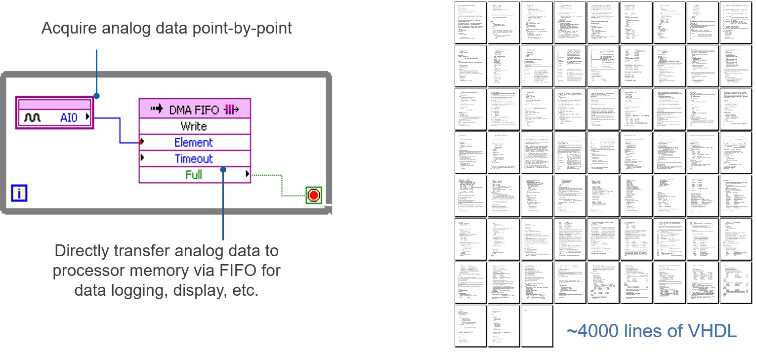
Figure 10: On the left is LabVIEW, which is a high-level design tool for FPGAs. It provides abstraction for the low-level complexity often found when creating and scaling VHDL designs.
Then to simulate and verify the behavior of your FPGA logic, LabVIEW offers features directly in the development environment. Without knowledge of the low-level HDL language, you can create test benches to exercise the logic of your design. In addition, the flexibility of the LabVIEW environment helps more advanced users model the timing and logic of their designs by exporting to cycle-accurate simulators such as Xilinx ISim.
LabVIEW FPGA compilation tools automate the compilation process, so you can start the process with a click of a button and receive reports and errors, if any, as compilation stages are completed. If timing errors do occur because of your FPGA design, LabVIEW highlights these critical paths graphically to expedite the debugging process.
Conclusion
The adoption of FPGA technology continues to increase as higher-level tools such as LabVIEW are making FPGAs more accessible. It is still important, however, to look inside the FPGA and appreciate how much is actually happening when block diagrams are compiled down to execute in silicon. Comparing and selecting hardware targets based on flip-flops, LUTs, multipliers, and block RAM is the best way to choose the right FPGA chip for your application. Understanding resource usage is extremely helpful during development, especially when optimizing for size and speed. This paper is not meant to be a comprehensive list of all FPGA fundamental building blocks. You can learn more about FPGAs and digital hardware design from the resources below.