Using the LabVIEW FPGA Desktop Execution Node
Overview
The LabVIEW FPGA Desktop Execution Node, available in FPGA simulation mode, enables you to create test benches with accurate timing characteristics. This tutorial introduces the concepts necessary to effectively use the FPGA Desktop Execution Node.
Note: The FPGA Desktop Execution Node is not available in a real-time environment.
Contents
- Understanding Simulated Time
- Example of Simple FPGA Acquisition and Processing
- Configuring the FPGA Desktop Execution Node
- Creating a Test Bench VI with the FPGA Desktop Execution Node
- Extending the FPGA Desktop Execution Node for Advanced Uses
- Additional Resources
Understanding Simulated Time
To effectively simulate an FPGA design using the FPGA Desktop Execution Node, you must understand two time paradigms, real-world time and simulated time.
Real-world time is the physical amount of time that elapses while something occurs. Because an FPGA is a programmable circuit, it takes a fixed amount of real-world time to execute such a circuit.
To simulate a design, you can create a model that reflects the functional behavior of the FPGA and execute this model on a computer processor. However, such a model does not have the same real-world timing as the FPGA. To create a model that has the same real-world timing as the FPGA, you must use simulated time.
Simulated time is an event-driven model of real-world time. When LabVIEW executes block diagram nodes, the execution causes simulated time to advance a certain number of steps. Clock ticks are the unit of simulated time where one clock tick is representative of a single cycle of the referenced FPGA clock.
What Nodes Advance Simulated Time?
Not all nodes on the FPGA block diagram advance simulated time. Table 1 shows the block diagram nodes that advance simulated time and the simulation time step they register.
Table 1. Block Diagram Nodes that Advance Simulated Time
| Block Diagram Node | Time Step1 |
| While Loop | Diagram execution time plus two ticks2 |
| Single-Cycle Timed Loop | 1 tick of the configured loop clock |
| Wait Express VI | User specified (ms, us, or ticks) |
| Loop Timer Express VI | User specified (ms, us, or ticks)3 |
| FIFOs (except DMA) | User specified (ticks) |
| Wait on Occurrence VI | User specified (ms or ticks) |
| Interrupt VI4 | One tick repeated until the interrupt is cleared |
1All time step behavior is relative to the top-level clock unless otherwise noted.
2The time step behavior of the While Loop is subject to change with each version of LabVIEW.
3The Loop Timer Express VI registers for the difference between the user-specified time step and the loop execution time step
4This only applies when you set the Wait Until Cleared input of the Interrupt VI to TRUE
Calculating Simulated Time
To fully understand how different parts of your LabVIEW FPGA code will interact with one another in simulation mode, you must calculate their impact on simulated time.
Using the details in table 1, you can manually inspect and calculate the simulated time step for a block diagram. Figure 1 shows an example VI that uses a 40 MHz top-level clock.
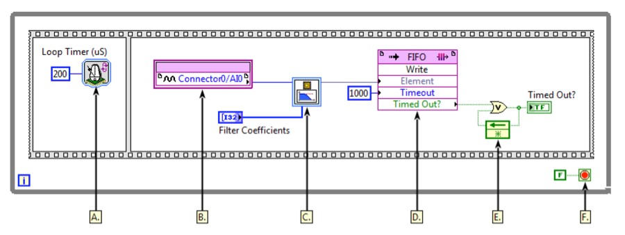
Figure 1. Example FPGA VI (40 MHz Top-Level Clock)
The following list describes important details about Figure 1.
A. The Loop Timer Express VI registers for a time step of 200 us, which is 8,000 ticks of the top-level clock, minus the time step of the rest of the While Loop.
B. The analog input, which is an FPGA input, does not register for any time step in simulation mode. FPGA output has the same behavior.
C. The Butterworth Filter Express VI contains a 40 MHz single-cycle timed loop that iterates once per call. Therefore, this express VI registers for a time step of 1 tick.
D. The target-scoped FIFO only registers for a time step of 1,000 ticks if the FIFO is timed out. Otherwise, no time step is registered.
E. Basic block diagram nodes including logic and math functions do not register for a simulation time step.
F. The While Loop registers for a time step of two ticks of the top-level clock.
Considering that manually calculating the simulated time step of a block of code is not always practical or necessary, you can calculate the simulated time step by using the Tick Count Express VI to benchmark the simulation execution time. Figure 2 shows the previous example VI instrumented to calculate the entire loop time step.
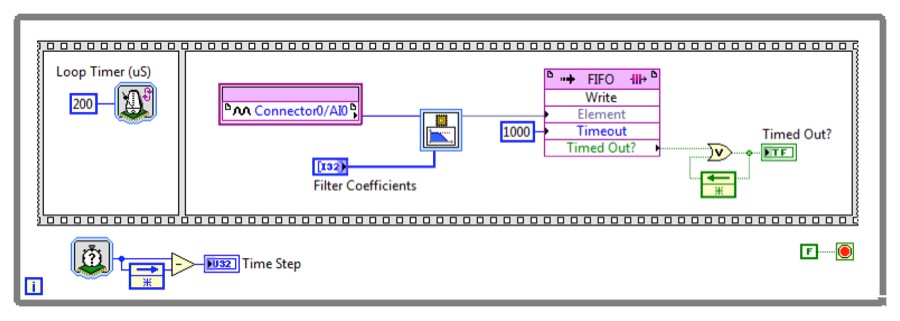
Figure 2. Example FPGA VI With Time Step Counter
The example VIs shown in Figure 1 and Figure 2 always execute with a simulated time step of 8,000 ticks, which equals 200 us, yielding a loop rate of 5 kHz. The Loop Timer Express VI applies a variable time step to enforce consistent timing between loop iterations, as shown in Table 2.
Table 2. Comparing Time Steps
| Time Step | ||
| Loop and Diagram | Loop Timer Express VI | |
| When Timed Out? of the FIFO Write method returns FALSE | 3 Ticks | 7,997 Ticks |
| When Timed Out? of the FIFO Write method returns TRUE | 1,003 Ticks | 6,997 Ticks |
Enforcing Accurate Simulated Time
In real-world time (FPGA execution mode), every node on the FPGA block diagram is represented by some physical circuitry and takes time to execute. In simulated time (FPGA simulation mode), only some nodes advance time. Because of this difference in the time paradigms, you must properly enforce simulated timing so the simulation behaves like FPGA execution. Figure 3 shows an example without properly enforced simulated timing.
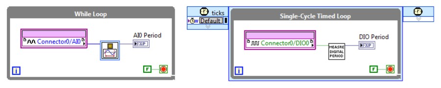
Figure 3. Example Without Proper Enforcement of Simulated Time
The example in Figure 3 contains two independent loops, which both run on the 40 MHz top-level clock. Table 3 analyzes the real-world and simulated timing of both loops.
Table 3. Timing Analysis of Figure 3
| Real-World Time | Simulated Time | |
| While Loop | 183 ticks | 12 ticks |
| Single-Cycle Timed Loop | 1 tick | 1 tick |
Notice that the real-world time and simulated time for the While Loop in Figure 3 are not equivalent. In real-world time, the single-cycle timed loop (SCTL) iterates 183 times faster than the While Loop, whereas in simulation mode, the SCTL iterates only 12 times faster than the While Loop.
This is because the While Loop does not contain any nodes to enforce timing in simulation mode. While it is acceptable not to specify timing for a While Loop, adding a Loop Timer Express VI allows more accurate control of the execution time and makes simulation timing accurate to real-world timing. Figure 4 shows an example VI, modified based on the previous example, that contains a Loop Timer Express VI.
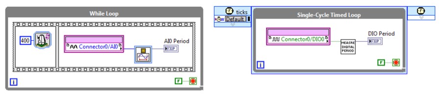
After adding a Loop Timer Express VI with a value greater than or equal to the real-world time to the While Loop, the simulation timing and real-world timing of the While Loop are equivalent. FPGA code with parallel data paths or loops will not simulate accurately relative to each other unless simulated time is properly enforced.
Example of Simple FPGA Acquisition and Processing
Now that you have a good understanding of simulated time, you can learn to effectively use the FPGA Desktop Execution Node. The remainder of this tutorial will focus on the testing the example FPGA code in Figures 5 and 6.
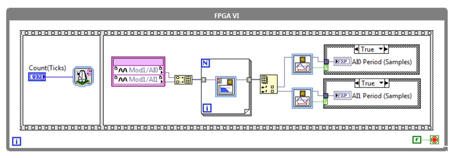
Figure 5. Example FPGA VI
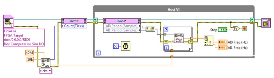
The FPGA VI in Figure 5 acquires two channels of analog input data, applies a 10 kHz lowpass Butterworth filter, and then easures the period of each signal. The corresponding host VI in Figure 6 sets the loop time and then periodically reads and scales the FPGA measurements.
In this example, we will replace the host VI with an FPGA Desktop Execution Node to create a test bench. Using the test bench, you can apply customized test vectors to FPGA inputs, capture FPGA output values, and validate code functionality.
Configuring the FPGA Desktop Execution Node
This section explains the FPGA Desktop Execution Node configuration options and provides related considerations. Placing an FPGA Desktop Execution Node on the block diagram of your RT of Host VI will automatically launch the configuration dialog box, as shown in Figure 7.
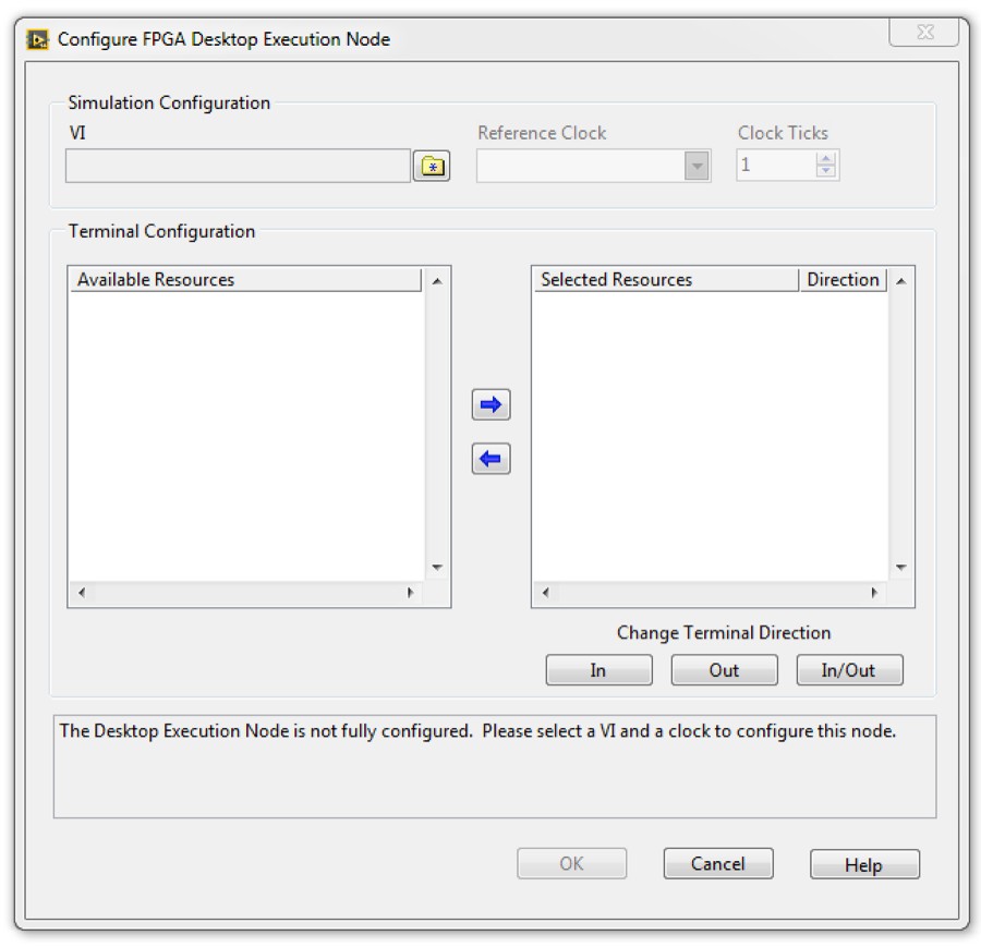
Figure 7. FPGA Desktop Execution Node Configuration Dialog
Simulation Configuration
The following configuration options in the Simulation Configuration section specify how the FPGA Desktop Execution Node behaves with respect to simulated time.
- VI – This option specifies the FPGA VI to run. Click the Browse VI button to display the Select VI dialog box and select the VI you want to reference. You can select any FPGA VI in the LabVIEW project as the target for the FPGA Desktop Execution Node.
- Reference Clock - This option specifies an available FPGA clock to use as the timing source for simulated time. You can select any top-level or derived clock in your LabVIEW project as the reference clock.
- Clock Ticks- This option specifies the number of clock ticks to run the FPGA VI for each call to the FPGA Desktop Execution Node. You must specify a non-zero integer.
For our example, we will use the 40 MHz onboard clock as a reference. The loop in our example runs at 50 kHz that equals 800 ticks of the 40 MHz clock and we desire to provide stimulus to the FPGA VI in every loop iteration. Therefore, we will set the FPGA Desktop Execution Node to 800 clock ticks.
Terminal Configuration
After you have targeted a VI for the FPGA Desktop Execution Node, the Available Resources option displays a list of I/O resources and front panel controls and indicators available for simulating with the FPGA Desktop Execution Node. Figure 8 shows the available resources for our example.
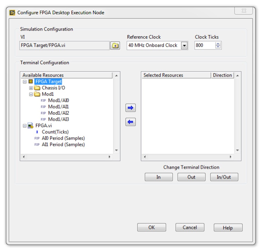
Figure 8. Example FPGA VI Resources Available in the Desktop Execution Node
In our test bench VI, we will set the loop period with the Count (Ticks) control and provide custom stimulus to Mod1/AI0 and Mod1/AI1. As we provide stimulus to these resources, we will analyze the output of AI0 Period (Samples) and AI1 Period (Samples).
Using the arrow and terminal direction controls, we can configure these resources to appear as terminals on the FPGA Desktop Execution Node. Figure 9 shows the selected resources for our example.
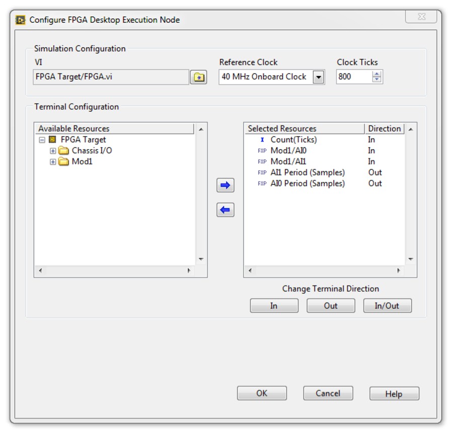
Figure 9. Example of Selected FPGA VI Resources
Creating a Test Bench VI with the FPGA Desktop Execution Node
Now that you have configured the FPGA Desktop Execution Node, you can use this node to create a test bench VI to verify the functionality of our FPGA VI. Let’s start by putting the FPGA Desktop Execution Node into a While Loop with a stop control and some loop timing, as shown in Figure 10. Using a loop timer in the test bench VI helps prevent CPU overload but has no affect on FPGA simulated time.
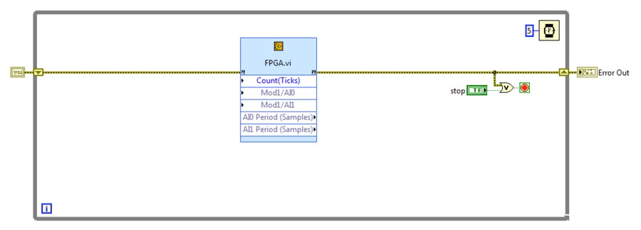
Figure 10. Putting the FPGA Desktop Execution Node in a While Loop
Setting FPGA VI Parameters
If your host VI has code that is used to calculate and set FPGA VI parameters, you can typically reuse that code in your FPGA Desktop Execution Node test bench VI. Figure 11 shows that the loop timer calculation code is reused.
Note that the FPGA Desktop Execution Node was configured specifically for the 50 kHz loop rate. If you change the loop rate value, you must evaluate how FPGA simulated time is affected and adjust the FPGA Desktop Execution Node settings accordingly.
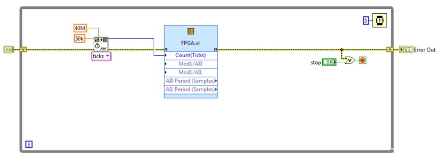
Figure 11. Reused Loop Timer Scaling Code
Generating Custom Input Vectors
One of the most powerful features of the FPGA Desktop Execution Node is the ability to stimulate FPGA input with a custom input vector. Figure 12 shows how to use the Signal Generation PtByPt VIs to create adjustable input waveforms for Mod1/AI0 and Mod1/AI1.
The FPGA Desktop Execution Node supports only the scalar data type. However, you can use a variety of techniques to generate point-by-point input vectors. Another common practice is to create a set of reusable input vectors by generating and saving to unique files. You can then use the File input VIs to read a particular vector and apply it to the FPGA Desktop Execution Node. To see an example with input vectors from files, launch the NI Example Finder by selecting Help»Find Examples in LabVIEW 2015 or later, search for “Simulating Analog Signals with the Desktop Execution Node”, and open Simulating Analog Signals with the DEN.lvproj.
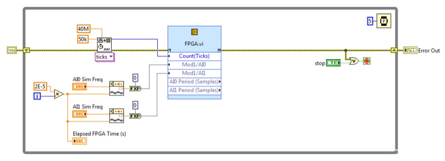
Figure 12. Generating Adjustable Input Waveforms
Collecting and Analyzing Output Vectors
For this simple example we use the FPGA Desktop Execution Node to read the FPGA indicators for AIO and AI1 Period (Samples). In Figure 13 we use the same scaling code as the original host VI and obtain frequency measurement for both channels.
The FPGA Desktop Execution Node enables you to analyze output vectors using any of the desktop LabVIEW function palettes and to display the output vectors using the full palette of front panel indicators.
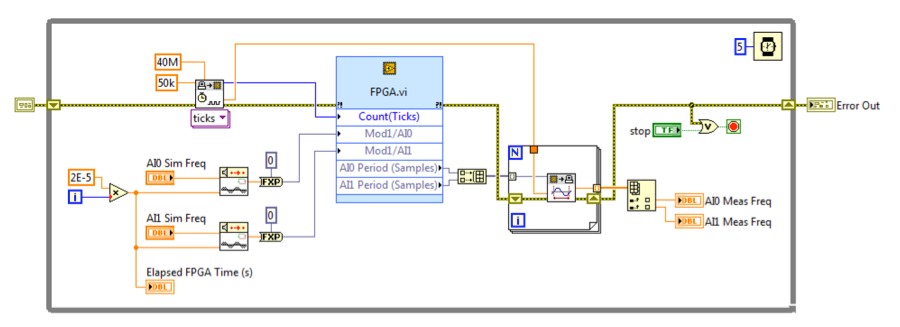
Figure 13. Obtaining Frequency Measurement
Extending the FPGA Desktop Execution Node for Advanced Uses
This tutorial introduces you with a basic understanding of how to create test benches by using the FPGA Desktop Execution Node. However, you can extend the FPGA Execution Node to address more advanced use cases.
FPGA applications that use DMA to transfer data to or from a host, and applications with large, complex host VIs require a different approach to the FPGA Desktop Execution Node. In these situations, you can use the FPGA Desktop Execution Node in parallel with the existing host VI. For an example of this use case, launch the NI Example Finder by selecting Help»Find Examples in LabVIEW 2015 or later, search for “Simulating Analog Signals with the Desktop Execution Node”, and open Simulating Analog Signals with the DEN.lvproj.
Another advanced use case is a simulation of VIs containing several loops running at different rates. Such a simulation requires additional considerations for simulation timing and FPGA Desktop Execution Node configuration. For an example of this use case, launch the NI Example Finder by selecting Help»Find Examples in LabVIEW 2015 or later, search for “Simulating Digital Signals with the Desktop Execution Node”, and open Simulating Digital Signals with the DEN.lvproj.