Using I2C with LabVIEW and the USB-845x
Overview
This page provides an overview of the USB-845x and how to use it with NI LabVIEW. This guide requires the installation of LabVIEW and the NI-845x Driver Software.
Contents
Using the USB-845x LabVIEW API with I2C
The USB-845x can be physically located more closely to I2C/SPI devices than PCI interfaces, reducing I2C bus length and minimizing noise problems. Additionally, the interface provides +5 V and GND to power circuits up to 230 mA with no external power supply.
Device Addressing
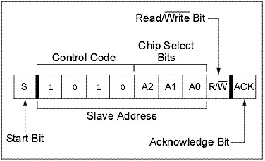
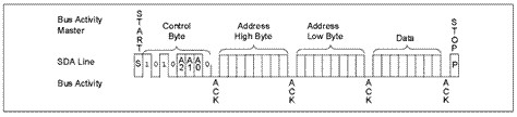
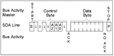
A control byte is the first byte received following the Start condition from the master device. The control byte consists of a 4-bit control code, typically set as ‘1010’ binary for read and write operations. The next three bits of the control byte are the Chip Select bits (A2, A1 and A0).
The Chip Select bits allow the use of up to eight devices on the same bus and are used to select which device is accessed. The Chip Select bits in the control byte must correspond to the logic levels on the corresponding A2, A1 and A0 pins for the device to respond. These bits are in effect the three Most Significant bits of the word address.
The last bit of the control byte defines the operation to be performed. When set to a one a read operation is selected and when set to a zero a write operation is selected.
Example of the control byte format
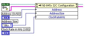
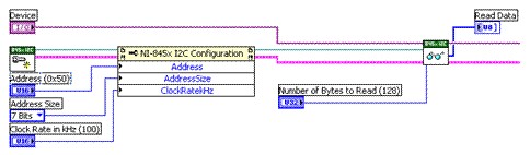
Basic LabVIEW API for Device Addressing
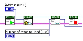
Use the property node to define the device address. If only one slave is connected to CS 0 the address is typically h50 (1010000- see control byte format above). The configuration output goes then to the high level Write, Read or Write/ Read VIs.
Property Node for 845x Basic API
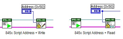
Advanced LabVIEW API for Device Addressing
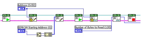
Use the Script Address + Write or + Read Functions after a Script Issue Start function to program the device address.
Write Operation
Byte Write
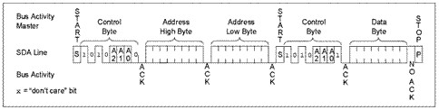
Following the Start condition from the master, the control code (four bits), the Chip Select (three bits) and the R/W bit (which is logic low for write operations) are clocked onto the bus by the master transmitter. This indicates to the addressed slave receiver that the address byte (for single address byte) or bytes (for two address bytes) will follow after it has generated an ACK bit during the ninth clock cycle.
Therefore, the next byte transmitted by the master is the high byte of the word address and will be written into the Address Pointer. The next byte is the Low Address Byte. After receiving another ACK, the master device will transmit the data word to be written into the addressed memory location. The slave ACKs again and the master generates a Stop condition. This initiates the internal write cycle (from the buffer to the memory) and during this time, the Slave will not generate ACK signals.
Example of a Byte Write
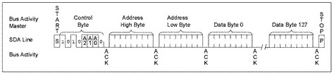
Page Write
The write control byte, word address and the first data byte are transmitted to the slave receiver in the same way as in a Byte Write. But instead of generating a Stop condition, the master transmits up to 127 additional bytes, which are temporarily stored in the on-chip page buffer and will be written into memory after the master has transmitted a Stop condition. After receipt of each word, the seven lower Address Pointer bits are internally incremented by one. If the master should transmit more than 128 bytes prior to generating the Stop condition, the address counter will roll over and the previously received data will be overwritten. As with the Byte Write operation, once the Stop condition is received, the internal write cycle will begin (from the page buffer to the memory). Refer to Figure 8 for an example of a Page Write.
Example of a Page Write
Note: You need to look at the page size of your chip!
Page Write operations are limited to writing bytes within a single physical page, regardless of the number of bytes actually being written. Physical page boundaries start at addresses that are integer multiples of the page buffer size (or ‘page size’) and end at addresses that are integer multiples of [page size – 1].
If a Page Write command attempts to write across a physical page boundary, the result is that the data wraps around to the beginning of the current page (overwriting data previously stored there), instead of being written to the next page as might be expected. It is therefore necessary for the application software to prevent page write operations that would attempt to cross a page boundary.
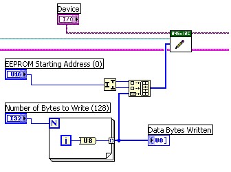
Basic LabVIEW API for Write Operations
The basic write operation takes the device descriptor, the configuration reference (including the device address) and uses a data byte array to write the data bytes to the address specified in the first two bytes.
The write functions acts like it is described above. To write to single byte addresses use a U8 integer instead of the U16 for the first data byte.
Example of 845x Basic API Write Operation
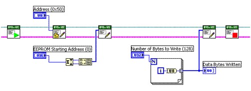
Advanced LabVIEW API for Write Operations
Use the Script write function twice to write the EEPROM Start address and the data bytes, followed by the Issue Stop function to have the same result as using the basic function.
Example of 845x Advanced API Write Functions
Read Operation
Read operations are initiated in the same way as write operations with the exception that the R/W bit of the control byte is set to ‘1’. There are three basic types of read operations: current address read, random read, and sequential read.
Current Address Read
The slave normally contains an address counter that maintains the address of the last word accessed, internally incremented by ‘1’. Therefore, if the previous read access was to address ‘n’ (n is any legal address), the next Current Address Read operation would access data from address n + 1. Upon receipt of the control byte with R/W bit set to ‘1’, the slave issues an ACK and transmits the 8-bit data word. The USB-845x will not ACK the transfer but does generate a Stop condition and the Slave discontinues transmission.
Example of Current Address Read Operation
Random Read
Random Read operations allow the USB-845x to access any memory location in a random manner. To perform this type of read operation, first the word address must be set. This is done by sending the word address to the slave as part of a write operation (R/W bit set to ‘0’). After the word address is sent, the master generates a Start condition following the ACK. This terminates the write operation, but not before the internal Address Pointer is set. Then, the master issues the control byte again but with the R/W bit set to a one.
The slave will then issue an ACK and transmit the 8-bit data word. The USB-845x will not ACK the transfer but does generate a Stop condition which causes the Slave to discontinue transmission. After a Random Read command, the internal address counter will point to the address location following the one that was just read.
Example of Random Read
Sequential Read
Sequential Reads are initiated in the same way as a Random Read except that after the slave transmits the first data byte, the master issues an ACK as opposed to the Stop condition used in a Random Read. This ACK directs the slave to transmit the next sequentially addressed 8-bit word (Reference the Example of Random Read). Following the final byte transmitted to the master, the master will not generate an ACK, but will generate a Stop condition.
To provide Sequential Reads, a slave normally contains an internal Address Pointer which is incremented by one at the completion of each operation. This Address Pointer allows the entire memory contents to be serially read during one operation. The internal Address Pointer will automatically roll over from address FFFF to address 0000 if the master ACKs the byte received from the array address FFFF.
Example of Sequential Read
Basic API for Read Operations
For the Basic API, we have two different VIs to reflect two different ways to read data. The easiest way is to read the current address as described in the Read Operations section. Therefore you need to use the Read VI and the Read process starts at memory address ‘0’ and the next time behind the last address you read. This is because you do not specify which start address to use and the slave uses his address counter that maintains the address of the last word accessed.
Example of 845x Basic API Read for Current Address
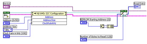
The second way to read data using I2C is using the Write/Read Function. For the Random and Sequentially Read this function performs a Write to specify the Start address to read from and a Read to read the data from this address. The Random Read reads only a single byte on a random position specified by the start address. The Sequentially Read reads as much data as specified with Number of Bytes to Read.
Example of 845x Basic API Read Write for Random and Sequentially Read Address
Advanced API for Read Operations
The 845x Advanced API allows you to script individual functions. For the Current Read, you have to write the address together with the read bit ‘1’, before you can read from the current address. For the Random and Sequentially Read you have to write the address and the write command bit ‘0’ before you can write the Start address. Then you have to write the address again together with the read bit ‘1’ to read any data. Both operations are separated by the Issue Start command.
Example of 845x Advanced API for Current Read
Example of 845x Advanced API for Random or Sequentially Read
Finding Examples
Where to find examples on a Windows XP system:
LabVIEW
Open LabVIEW » Help » Find Examples ... » Hardware Input and Output » I2C and SPICVI
C:\Program Files\National Instruments\CVIXX\samples\ni845x
Microsoft Visual C/C++ 6.0
C:\Program Files\National Instruments\NI-845x\MS Visual C\Examples
Note: To find the shipping examples on your computer, you will need to download the NI-845x Driver which can be found in the Related Links section.
SPI Bus
The SPI bus is a four-wire, full-duplex serial interface. Three of the wires, SCK, MOSI, and MISO, are shared along with a fourth wire, known as the chip select, which is a direction connection between the master and a single slave.
Communication across SPI uses a system known as data exchange. Whenever a bit is written to an SPI device across the MOSI lines, the SPI device concurrently returns a bit on the MISO line. Because data is transferred in both directions, it is up to the receiving device to know whether the received by is meaningful or not. For example, to receive data from an EEPROM, the master must configure the EEPROM to send n bytes of data and then must send n bytes to be exchanged for valid data. These bytes can usually be any value, and writing them serves only to clock the data out of the receiving device.
For more information, please review the following links:
NI USB-8451, Atmel AT25080A, and the LabVIEW SPI API
Using the NI USB-8451 SPI Interface to Evaluate a Texas Instruments Analog to Digital Converter