From Friday, April 19th (11:00 PM CDT) through Saturday, April 20th (2:00 PM CDT), 2024, ni.com will undergo system upgrades that may result in temporary service interruption.
We appreciate your patience as we improve our online experience.
From Friday, April 19th (11:00 PM CDT) through Saturday, April 20th (2:00 PM CDT), 2024, ni.com will undergo system upgrades that may result in temporary service interruption.
We appreciate your patience as we improve our online experience.
This guide provides information and guidance for migrating existing LabVIEW Communications 1.1 applications to LabVIEW Communications 2.0 for USRP Projects. If you prefer to migrate over an existing application, this guide addresses known issues that may arise in the process. It is recommended to start with a new project in 2.0 and duplicate the original project in the newer version.
This document covers LabVIEW Communications 1.1 to 2.0 Migration Guide for USRP Projects.
The guide is made up five documents covering the following topics:
Each section discusses the required steps to migrate that specific type of project. For example, if you would like to migrate a USRP streaming project, you should navigate to the USRP Projects section for guidance. If your project does not fall into the first three categories listed above, you should navigate to the General Projects section. Each section is meant to be self-contained and used independently of the others, so redundant information may be included in multiple sections.
Note: Always back up a copy of the original project before attempting any migration efforts.
This section describes the steps necessary for reusing a project that was initially based on the USRP API and example projects in LabVIEW Communications 2.0.
This section includes the following subsections. Use the one that is most appropriate for the type of USRP project you are migrating.
The USRP host-side API has several changes. When migrating code, this may cause VIs to be broken of functionality to be lost. Review the following items and make updates to the migrated code as needed.
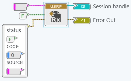
Figure 43: "niUSRP Open Rx Session.gvi" (1.1)
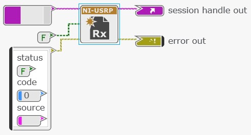
Figure 44: "niUSRP Open Rx Session.gvi" (2.0)
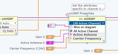
Figure 46: Drop Down Menu from Active Channel Filter
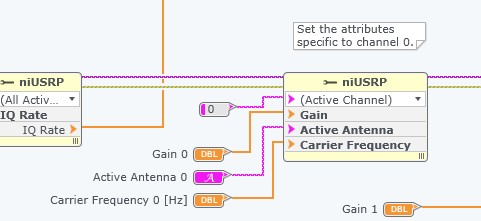
Figure 47: Corrected Active Channel Filter (No Longer Shows Exclamation or Error)
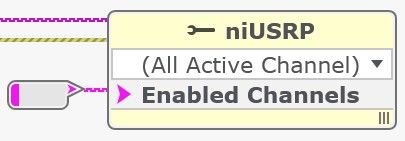
Figure 48: "Enabled Channels" Property (2.0)
Because the USRP interface (40 MHz BW) is deprecated with LabVIEW Communications 2.0, the new interface must now be used on the FPGA top-level. The new interface now handles both the 40 MHz BW and 120 MHz BW USRP models with the same interface. Hence, an FPGA bitfile rebuild is required.

Figure 51: Files to Delete from “USRP Resources.grsc”
Figure 52: Final “URSP Resources.grsc”
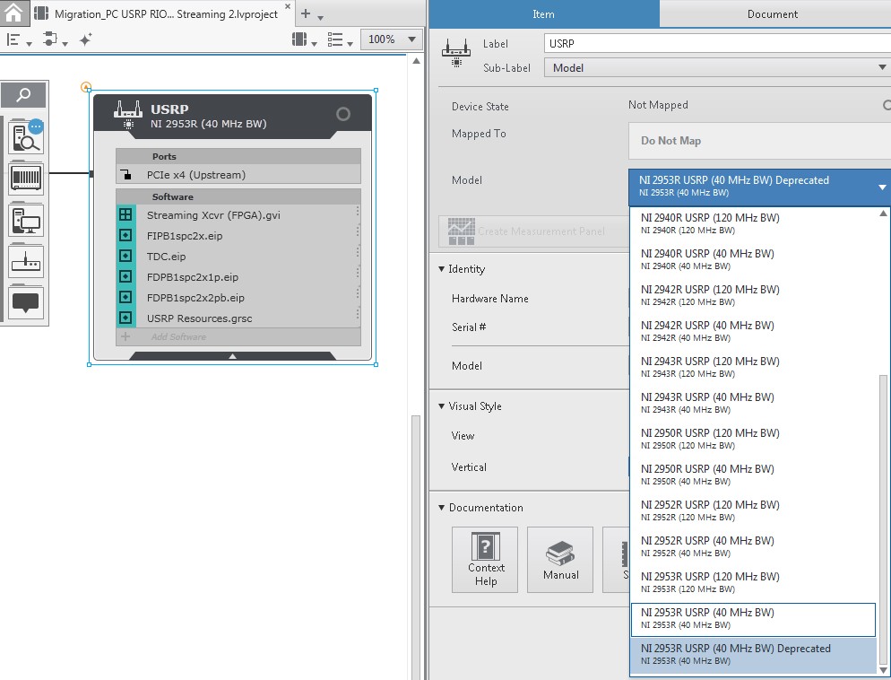
5. Select your USRP Target on the System Designer and change the "Model" in the right-hand rail to the non-deprecated version (ex: NI 2953R USRP (40 MHz BW) Deprecated » NI 2953R USRP (40 MHz BW)) as shown in Figure 53.
Figure 53: Select USRP Target from Right-Hand Rail
6. Generate a new 40 MHz Single-Device Streaming project in LabVIEW Communications 2.0 by navigating to New » Project Templates » USRP RIO 40 MHz BW Single-Device Streaming.
Note: This project will only be used to copy the necessary project files and code sections into the previous project that is being migrated.
7. Copy two VIs from the new project into the original project.
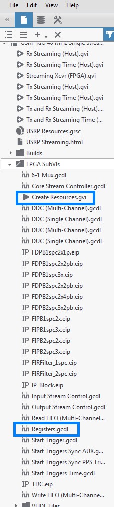
a. As shown in Figure 54, find the following subVIs from the <project directory>\FPGA SubVIs folder:
i. Create Resources.gvi
ii. Registers.gcdl
Figure 54: Files to Copy
b. Copy these on disk and paste to the same directory in the original project.
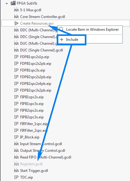
c. In the “Project Files” view on the Navigation Pane of the original project, the new files will appear slightly greyed out. Right-click on each and select Include as shown in Figure 55.
Note: Since the “Create Resources.gvi” is not a specific FPGA document (for example, CDL, MRD, and so on), there may be a prompt to select the target that the file should reside under. Select the same USRP target that your other files in this directory reside under.
Figure 55: Files to Include
8. In your original project, open the “Streaming Xcvr (FPGA).gvi”.
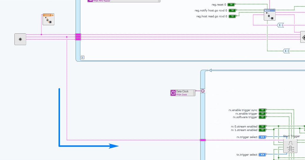
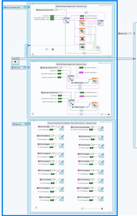
9. Find the three Clock-Driven Loops used for interfacing with the USRP and remove those loops as shown in Figure 56.
Figure 56: Clock Driven Loops
10. Open the “Streaming Xcvr (FPGA).gvi” of the new project.
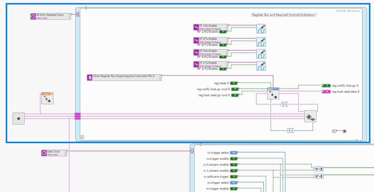
a. As shown in Figure 57, select and copy the following from the Diagram: “Create Resources.gvi”, “Process.gvi”, the Clock Constant, and the Clock-Driven Loop.
Figure 57: Clock-Driven Loop to Copy From
11. In the project you wish to migrate, paste the elements you copied from the new streaming project.
a. Rewire the “sync.resources” cluster wire from the “Create Recources.gvi” to the “Start Trigger.gcdl” as shown in Figure 58.
Figure 58: Rewire Cluster Wire to Start Trigger
12. Allow all document changes to finish loading and save all files.
13. Close the new streaming project as it is not needed anymore.
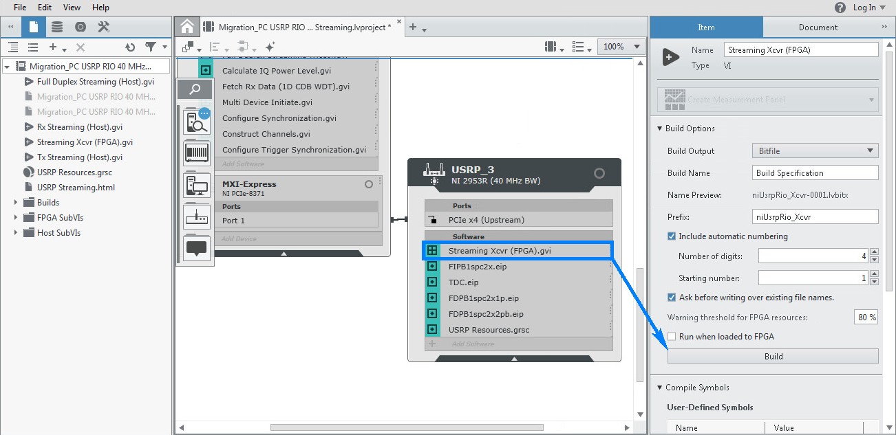
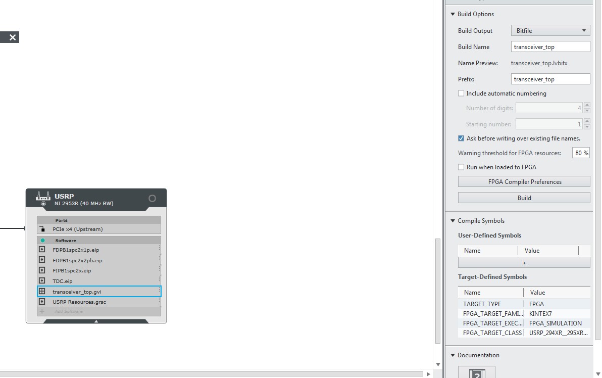
14. Compile the FPGA VI.
a. Open the System Designer (in the “Project Files” view of the Navigation Pane on the left) by double-clicking on the top project file.
b. Select the FPGA top-level under the target you want to build the bitfile for.
c. Click Build on the right pane as shown in Figure 59.
Figure 59: Compile the Project
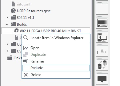
15. (Recommended) Once the bitfile is finished building, exclude it from the project as shown in Figure 60 and include it again. This will ensure that the latest changes are actually applied.

Figure 60: Option to Exclude Bitfile
The FIFO resource names in the Host subVIs that interface with DMA FIFOs must be updated. This includes VIs which aren't in VI.lib (Sample Project VIs and User VIs). In LabVIEW Communications 2.0, the FIFO resource contains additional prefixes for the FPGA resource file name along with the FIFO name itself. For example, “Rx Stream 0” becomes “USRP Resources.grsc\Rx Stream 0.” All FIFO node instances (Start/Stop, Configure, and Read/Write), along with any FPGA reference terminals, must be updated.
Use your newly compiled bitfile from step 14 above to get access to the DMA FIFO references required.
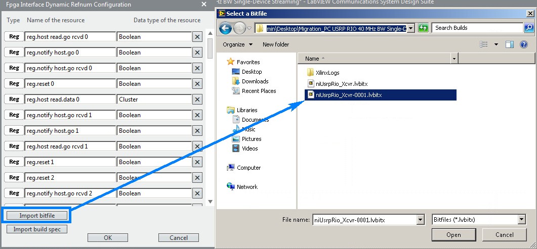
Figure 61: Right-Hand Rail Configure Option
i. In the “FPGA Interface Dynamic Refnum Configuration“ dialog, click Import bitfile and browse to your recently compiled bitfile.
Note: The default location will be in the <project directory>\Builds folder but this, along with the file name, will vary based on the configuration of the build spec used during compile.
ii. (Optional) With the “FPGA Interface Dynamic Refnum Configuration“ dialog still open, remove all unused resources by clicking the X symbol on the right side.
Note: This will not affect functionality but may make it easier to view used resources at a later time.
iii. Click OK in the “FPGA Interface Dynamic Refnum“ dialog.
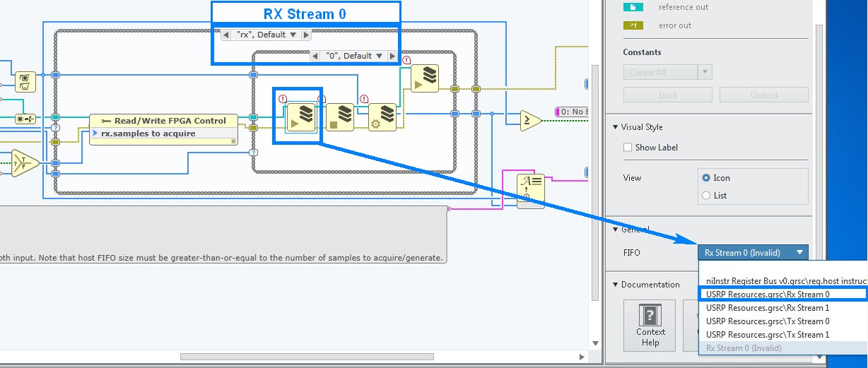
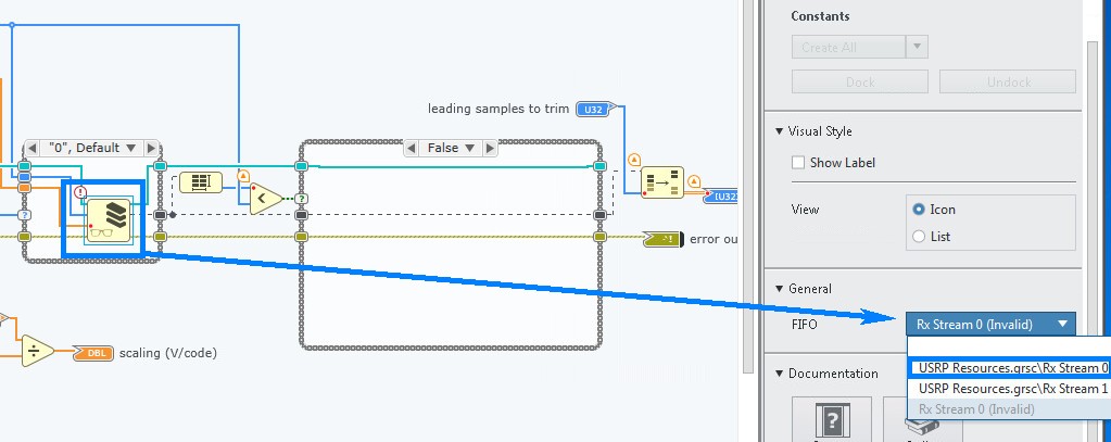
b. Update to the new DMA FIFO's in each Case Structure for each “rx” and “tx” case that contains a nested Case Structure for Stream, 0 and 1. Each case will contain one, or more, FIFO nodes of a Start DMA FIFO, Stop DMA FIFO, and Configure DMA FIFO. Using the right-hand rail configuration, update each FIFO node to the following:
i. Rx Stream 0 » USRP Resources.grsc\Rx Stream 0
ii. Rx Stream 1 » USRP Resources.grsc\Rx Stream 1
iii. Tx Stream 0 » USRP Resources.grsc\Tx Stream 0
iv. Tx Stream 1 » USRP Resources.grsc\Tx Stream 1
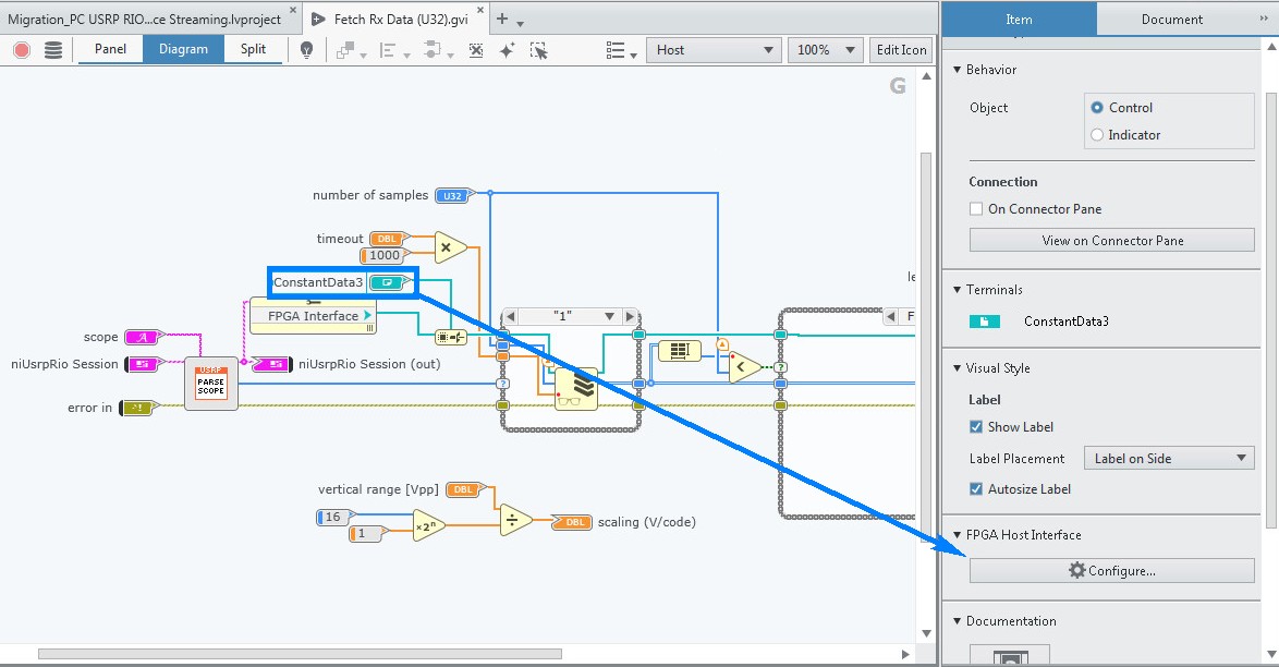
2. Follow the same general steps from step 1 for the "Fetch Rx Data (U32).gvi" in the <project directory>\Host SubVIs folder of your project.
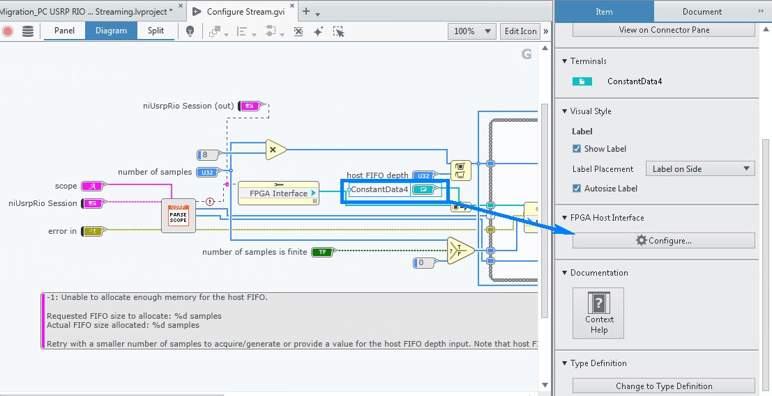
a. Select "ConstantData3" and click Configure in the right-hand rail as shown in Figure 64.
Figure 64: Configure Dialog in Right-Hand Rail
b. Click Import bitfile and browse to your recently compiled bitfile. Click OK.
c. Update the left-most Case Structure’s Read DMA FIFO to point at the new DMA FIFO's for both cases. Change this by going to the right-hand rail configuration. Update the following:
i. Rx Stream 0 » USRP Resources.grsc\Rx Stream 0
ii. Rx Stream 1 » USRP Resources.grsc\Rx Stream 1
Figure 65: Update Read DMA FIFO
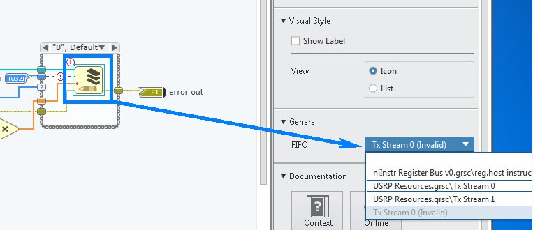
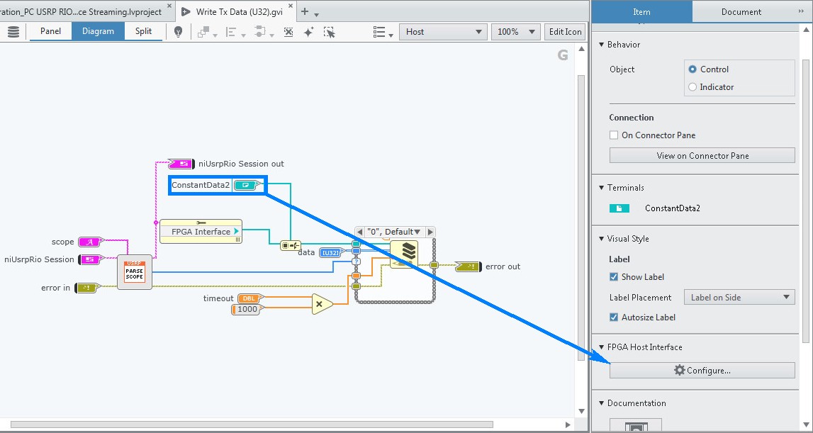
3. Follow the same general steps from step 1 and step 2 for the "Write Tx Data (U32).gvi" in the <project directory>\Host SubVIs folder of your project.
a. Select "ConstantData2" and click Configure in the right-hand rail.
Figure 66: Configure Dialog in Right-Hand Rail
b. Click Import bitfile and browse to your recently compiled bitfile. Click OK.
c. Update the Case Structure’s Write DMA FIFO to point at the new DMA FIFO's for each case. Change this by going to the right-hand rail configuration. Update the following:
i. Tx Stream 0 » USRP Resources.grsc\Tx Stream 0
ii. Tx Stream 1 » USRP Resources.grsc\Tx Stream 1
Figure 67: Update Write DMA FIFO
Note: Similar changes must be made if any DMA FIFO's were added to the project in previous versions of LabVIEW Communications.
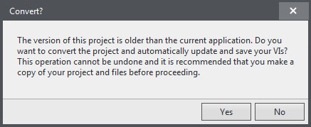
Figure 68: Convert Dialog
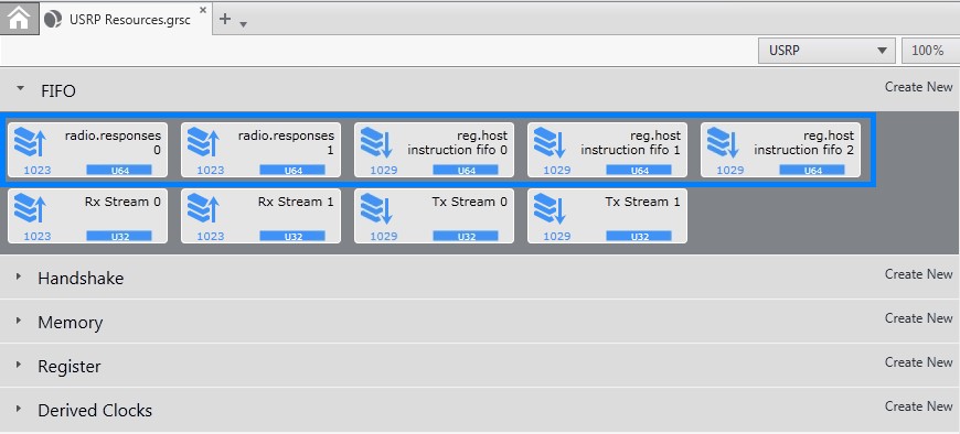
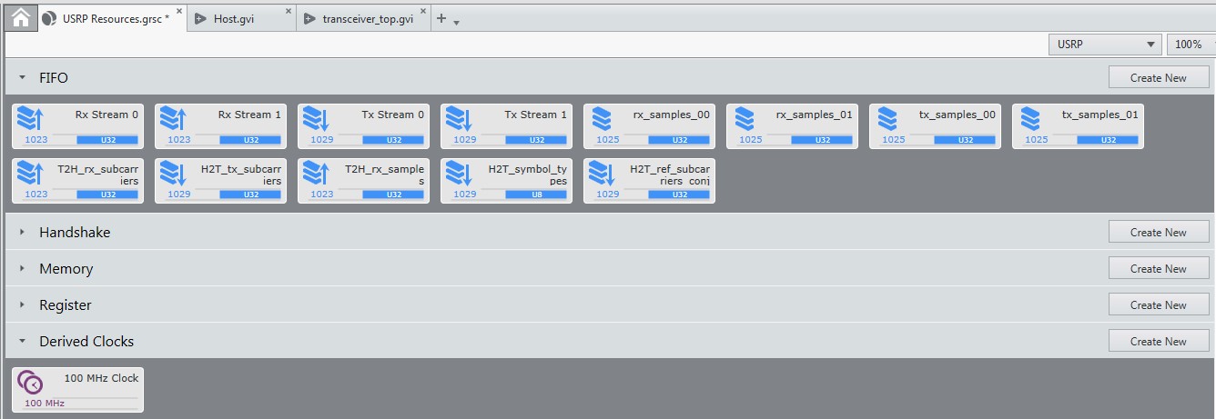
4. Delete the following items from “USRP Resources.grsc”:
a. radio.responses 0
b. radio.responses 1
c. reg.host instruction fifo 0
d. reg.host instruction fifo 1
e. reg.host instruction fifo 2
Figure 69: Items to Delete from “USRP Resources.grsc”
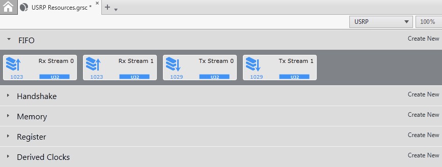
Figure 70: Corrected “USRP Resources.grsc”
5. Open the “Streaming Xcvr (FPGA).gvi” of the new project.
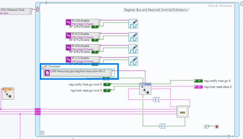
6. Change the DMA FIFO reference going into the “Process.gcdl” by clicking the IO Constant drop-down. From that drop-down menu, select “niInstr Register Bus v0.grsc\reg.host instruction fifo 0”.
Figure 71: Change DMA FIFO Reference
7. Compile the FPGA VI.
a. Open the System Designer (in the “Project Files” view of the Navigation Pane on the left) and double-click on the top-most project file.
b. Select the FPGA top-level under the target you want to build the bitfile for.
c. Click Build on the right-hand rail as shown in Figure 72.
Figure 72: Compile FPGA VI by Clicking Build
8. (Recommended) Once the bitfile is finished building, exclude it from the project as shown in Figure 73 and include it again. This will ensure that the latest changes are actually applied.
Figure 73: Exclude File
Follow the same steps listed in the PC/PXIe 40 MHz USRP RIO Single and Multi-Device Host-Side section.
Because the USRP interface (40 MHz BW) is deprecated with LabVIEW Communications 2.0, the new interface must now be used on the FPGA top-level. The new interface now handles both the 40 MHz BW and 120 MHz BW USRP models with the same interface. Hence, an FPGA bitfile rebuild is required.
Figure 74: Convert Dialog
4. Delete the following items from “USRP Resources.grsc”:
a. radio.responses 0
b. radio.responses 1
c. reg.host instruction fifo 0
d. reg.host instruction fifo 1
e. reg.host instruction fifo 2
Figure 75: Final “URSP Resources.grsc”
5. Select your USRP Target on the System Designer and change the "Model" in the right-hand rail to the non-deprecated version (ex: NI 2953R USRP (40 MHz BW) Deprecated » NI 2953R USRP (40 MHz BW)) as shown in Figure 76.
Figure 76: Select USRP Target from Right-Hand Rail
6. Generate a new SISO TDD OFDM project by navigate to Learning » Hardware Input and Output » NI USRP RIO » SISO TDD OFDM on NI USRP RIO.
Note: This project will only be used to copy the necessary project files and code sections into the previous project that is being migrated.
7. Copy two VIs from the new project into the original project.
a. As shown in Figure 77, find the following subVIs from the <project directory>\PXIe USRP RIO Streaming \FPGA SubVIs\ folder:
i. Create Resources.gvi
ii. Registers.gcdl
Figure 77: Files to Copy
b. Copy these on disk and paste to the directory in the original project: <project directory>\PXIe USRP RIO Streaming\FPGA SubVIs
c. In the “Project Files” view on the Navigation Pane of the original project, the new files will appear slightly greyed out. Right-click on each and select Include as shown in Figure 78.
Note: Since the “Create Resources.gvi” is not a specific FPGA document (for example, CDL, MRD, and so on), there may be a prompt to select the target that the file should reside under. Select the same USRP target that your other files in this directory reside under.
Figure 78: Files to Include
8. In the original project, open the “transceiver_top.gvi”.
9. Find the three Clock-Driven Loops used for interfacing with the USRP and remove those loops as shown in Figure 79.
Figure 79: Clock Driven Loops
10. Open the “Streaming Xcvr (FPGA).gvi” of the new project.
a. As shown in Figure 80, select and copy the following from the Diagram: “Create Resources.gvi”, “Process.gvi”, the Clock Constant, and the Clock-Driven Loop.
Figure 80: Clock-Driven Loop to Copy From
11. In the project you wish to migrate, paste the elements you copied from the new sample streaming project.
a. Rewire the “sync.resources” cluster wire from the “Create Recources.gvi” to the “Start Trigger.gcdl” as shown in Figure 81.
Figure 81: Rewire Cluster Wire to Start Trigger
12. Allow all document changes to finish loading and save all files.
13. Close the new project as it is not needed anymore.
14. Compile the FPGA VI.
a. Open the System Designer (in the “Project Files” view of the Navigation Pane on the left) by double-clicking on the top project file.
b. Select the FPGA top-level under the target you want to build the bitfile for.
c. Click Build in the right-hand rail as shown in Figure 82.
Figure 82: Compile the Project
15. (Recommended) Once the bitfile is finished building, exclude it from the project as shown in Figure 83 and include it again. This will ensure that the latest changes are actually applied.
Figure 83: Option to Exclude Bitfile
The FIFO resource names in the Host subVIs that interface with DMA FIFOs must be updated. This includes VIs which aren't in VI.lib (Sample Project VIs and User VIs). In LabVIEW Communications 2.0, the FIFO resource contains additional prefixes for the FPGA resource file name along with the FIFO name itself. For example, “Rx Stream 0” becomes “USRP Resources.grsc\Rx Stream 0.” All FIFO node instances (Start/Stop, Configure, and Read/Write), along with any FPGA reference terminals, must be updated.
Use your newly compiled bitfile from step 14 above to get access to the DMA FIFO references required.
Figure 84: Right-Hand Rail Configure Option
i. In the “FPGA Interface Dynamic Refnum Configuration“ dialog, click Import bitfile and browse to your recently compiled bitfile.
Note: The default location will be in the <project directory>\Builds folder but this, along with the file name, will vary based on the configuration of the build spec used during compile.
ii. (Optional) With the “FPGA Interface Dynamic Refnum Configuration“ dialog still open, remove all unused resources by clicking the X symbol on the right side.
Note: This will not affect functionality but may make it easier to view used resources at a later time.
iii. Click OK in the “FPGA Interface Dynamic Refnum“ dialog.
b. Update to the new DMA FIFO's in each Case Structure for each “rx” and “tx” case that contains a nested Case Structure for Stream, 0 and 1. Each case will contain one, or more, FIFO nodes of a Start DMA FIFO, Stop DMA FIFO, and Configure DMA FIFO. Using the right-hand rail configuration, update each FIFO node to the following:
i. Rx Stream 0 » USRP Resources.grsc\Rx Stream 0
ii. Rx Stream 1 » USRP Resources.grsc\Rx Stream 1
iii. Tx Stream 0 » USRP Resources.grsc\Tx Stream 0
iv. Tx Stream 1 » USRP Resources.grsc\Tx Stream 1
2. Follow the same general steps from step 1 for the "Fetch Rx Data (U32).gvi" in the <project directory>\Host SubVIs folder of your project.
a. Select "ConstantData3" and click Configure in the right-hand rail as shown in Figure 87.
Figure 87: Configure Dialog in Right-Hand Rail
b. Click Import bitfile and browse to your recently compiled bitfile. Click OK.
c. Update the left-most Case Structure’s Read DMA FIFO to point at the new DMA FIFO's for both cases. Change this by going to the right-hand rail configuration. Update the following:
i. Rx Stream 0 » USRP Resources.grsc\Rx Stream 0
ii. Rx Stream 1 » USRP Resources.grsc\Rx Stream 1
Figure 88: Update Read DMA FIFO
3. Follow the same general steps from step 1 and step 2 for the "Write Tx Data (U32).gvi" in the <project directory>\Host SubVIs folder of your project.
a. Select "ConstantData2" and click Configure in the right-hand rail.
Figure 89: Configure Dialog in Right-Hand Rail
b. Click Import bitfile and browse to your recently compiled bitfile. Click OK.
c. Update the Case Structure’s Write DMA FIFO to point at the new DMA FIFO's for each case. Change this by going to the right-hand rail configuration. Update the following:
i. Tx Stream 0 » USRP Resources.grsc\Tx Stream 0
ii. Tx Stream 1 » USRP Resources.grsc\Tx Stream 1
Figure 90: Update Write DMA FIFO
4. Open the “FPGA Reference Cast.gvi”: <project directory>\Host\FPGA Reference Cast.gvi
a. Update the “transceiver_top” to use the newly compiled bitfile by going to configure and pointing it at the bitfile.
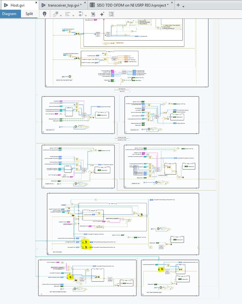
5. In the top-level VI, update all DMA FIFO References to use the new G Resource DMA FIFO Name. They are highlighted in yellow in Figure 91.
Figure 91: DMA FIFO References
Note: Similar changes must be made if any DMA FIFO's were added to the project in previous versions of LabVIEW Communications.
Continue onto other sections of the LabVIEW Communications 1.1 to 2.0 Migration Guide for:
The LabVIEW Communications product documentation provides detailed information in addition to the tasks discussed in this guide. Hardware manuals also contain valuable information about the features and performance characteristics of NI RIO devices.
The main NI support page, ni.com/support, provides quick access to manuals, KnowledgeBase documents, tutorials, example code, community forums, technical support, and customer service.