From Friday, April 19th (11:00 PM CDT) through Saturday, April 20th (2:00 PM CDT), 2024, ni.com will undergo system upgrades that may result in temporary service interruption.
We appreciate your patience as we improve our online experience.
From Friday, April 19th (11:00 PM CDT) through Saturday, April 20th (2:00 PM CDT), 2024, ni.com will undergo system upgrades that may result in temporary service interruption.
We appreciate your patience as we improve our online experience.
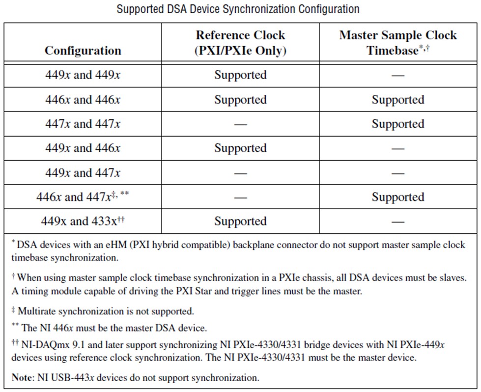
Many DSA applications require multiple input and output operations across numerous devices at the same time. Synchronizing these inputs and outputs ensures that the different operations are correlated in time. This facilitates the coordination or comparison of acquired and generated data signals with time. By synchronizing two or more devices, it is possible to extend the channel count of the DSA measurement system while still maintaining the high phase accuracy typically seen between channels on a single device. For a reference on basic synchronization terms, see the Synchronization Basics Dev Zone linked below.
Depending on your specific DSA hardware you will use either Sample Clock Timebase Synchronization or Reference Clock Synchronization. However, at the ADC level, both methods achieve synchronization by sharing a clock, synchronization pulse and start trigger.
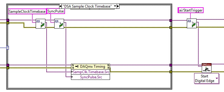
To configure a DSA measurement system synchronized on the Sample Clock Timebase, one “master” DSA device will export its Sample Clock Timebase signal to all other, “slave,” devices to be synchronized. The Sample Clock Timebase is a large multiple of the sample clock, and it can be as high as 26.2 MHz for some devices. Since this clock will be controlling the ADCs on all the devices, the relative phase of this signal is very important for synchronization.
For a PXI system, the master DSA device must be placed in the master timebase slot of the chassis, typically the second slot. The master DSA device must be placed in this slot in order to drive the PXI Star Trigger line of the chassis, a point-to-point routing line capable of increased synchronization performance – specifically a propagation delay of no more than 5 ns and an inter-module delay of no more than 1 ns.
Note: The master timebase synchronization method exposed is only valid if a PXI chassis used. If the chassis is PXIe, the DSA devices don't have access to the PXI Star lines. When using master sample clock timebase synchronization in a PXIe chassis, all DSA devices must be slaves.
A timing module capable of driving the PXI Star trigger lines must be the master. See Master Sample Clock Timebase Synchronization section in the NI Dynamic Signal Acquisition User Manual for more information.
The timebase synchronization signal generated by the master device in slot 2 will then be accessed by the other modules in the chassis through the backplane.
Note: That the master module can route the timebase synchronization signal on the PXI Star Trigger Lines for modules in slots 3-14.
The master device must also route a synchronization pulse to all slave boards; however, this can be done using any of the PXI trigger lines. This synchronization pulse will first reset the ADCs and DACs in the entire system at the same time, and then phase align all of the clocks on the board to within nanoseconds. Finally, a start trigger from one of the devices, not necessarily the master device, must be exported across one of the PXI trigger lines to the other devices in order to start acquiring on all boards simultaneously.
For a PCI system, the timebase synchronization signal, synchronization pulse, and start trigger will be routed on one of the lines of the RTSI cable connecting the devices of the system.
Note: that there are default lines for each of the three signals.
Figure 1: PXI, PXIe, and PCI Sample Clock Timebase Synchronization
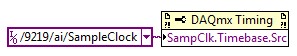
For a cDAQ system, Sample Clock Timebase Synchronization will be handled by the DAQmx driver, within the chassis (9178, 9174). Through channel expansion, the driver will automatically share a Sample Clock Timebase, Sync Pulse, and Start Trigger between the modules. For synchronization applications involving DSA modules with different timebases, DAQmx will arbitrarily choose a module with the fastest timebase as the timebase source for all the modules. If you wish to use the slower Sample Clock Timebase you may do so by specifying the Sample Clock Timebase Source property for the task.
Figure2: Sample Clock Timebase Property
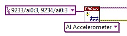
Figure 3: cDAQ Sample Clock Timebase Synchronization via Channel Expansion
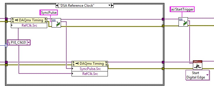
To configure a DSA measurement system synchronized on the Reference Clock, both master and slave devices will lock their ADCs or DACs over the sample clock to a shared reference clock on the PXI and PXIe chassis backplane. This shared reference clock is either the native 10 MHz reference clock on the PXI and PXIe chassis backplane (PXI_CLK10) or an external source driving the PXI_CLK10 line.
The PXI chassis supplies the clock to each peripheral slot, independently, driven by an independent buffer. This reference clock is accurate to 25 ppm, and can be overridden by another 10 MHz clock sourced by a capable PXI or PXIe module installed in the star trigger slot (slot 2) of the chassis. Driving the line with an external clock source will automatically disable the 10 MHz source generated on the chassis backplane. Master and slave devices can be placed in any slot, and all devices within the chassis can be synchronized by this method. An arbitrarily chosen master board issues a synch pulse on one of the PXI Trigger lines to reset the ADCs and DACs, and to reset the divide counter to phase align the clocks of the system to within nanoseconds. One DSA device (not necessarily the master) will export the start trigger on one of the PXI Trigger lines, forcing the synched devices to acquire or generate data simultaneously. The DSA devices that support this type of synchronization (see Table 1) contain phase-locked loop (PLL) circuitry that enables them to lock to the reference clock.
Figure 4: Reference Clock Synchronization